
No, it is a frustration with members of this forum, generally. You are just another log at times.
Here is the article:
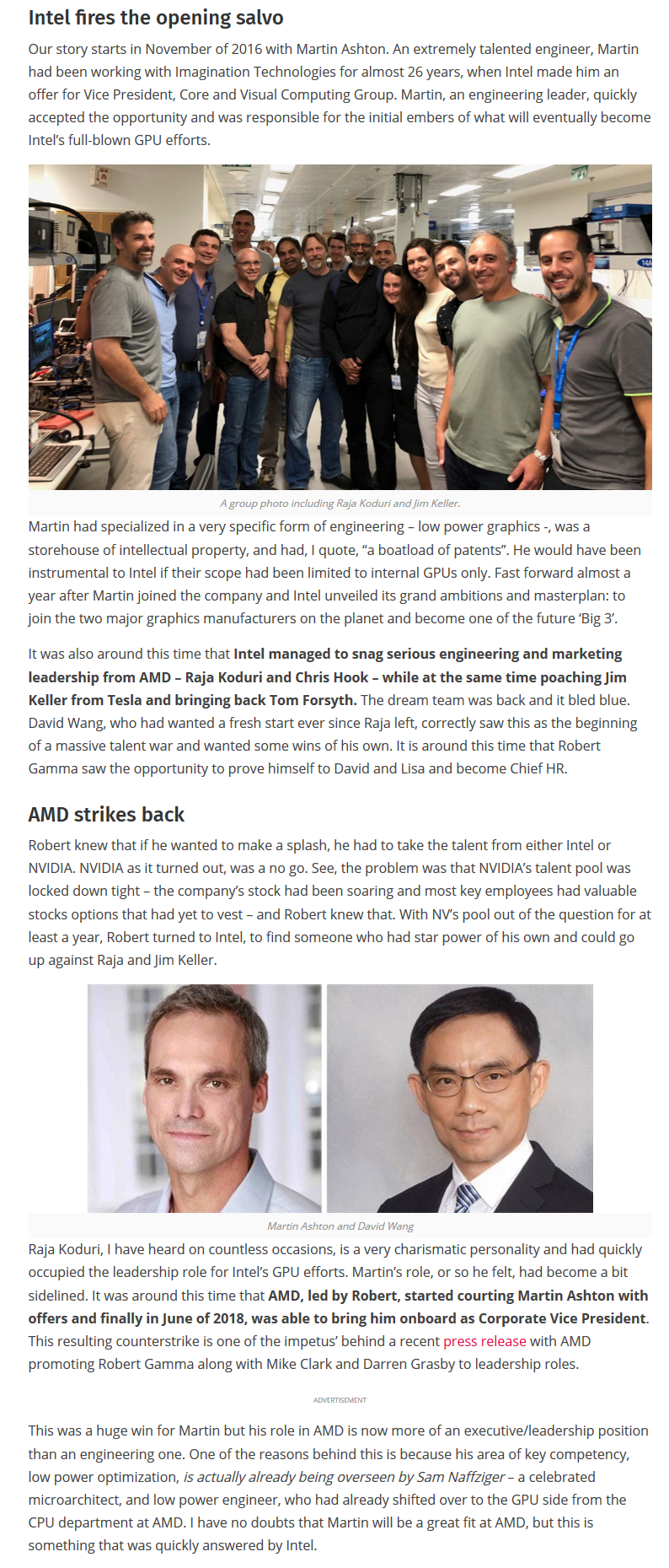
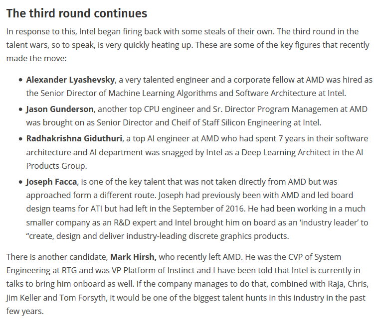
https://wccftech.com/intel-amd-talent-wars-heat/
Pouching talent isn't them leaving to find other work, it is being offered more to leave. Here is the list:
Notice that third round list: Machine learning algorithms and software, CPU engineer, AI engineer and deep learning architect, R&D expert for graphics that left AMD in 2016. These are a handful of engineers, literally (talking 4, while everyone expected Raja was going to be fired during his sabattical after the Vega flop, Chris was a marketer, Keller worked at Tesla in between and his entire M.O. was to work at a place and leave after the design work was complete, as seen FOR OVER 20 YEARS).
So, no, gaming is how you subsidize research and help do the bread and butter to a degree. SERVER is where the money is. Data centers. Hell, even mobile gaming and cloud gaming is being targeted in data centers. Who makes the AI? Data centers. What do corporations, universities, etc. do their research on? Data centers. How much of that is gaming oriented? What are the highest margin products? (hint: GV100, TU100, GP100, and AMD's server offerings).
So where is the "bunch of people"? That was done over YEARS. Designs of products take YEARS. New CPU architectures take YEARS. So nothing happening now was done in the past couple months, and Intel has been trying to correct course for awhile. Hiring the talent over these couple years, since 2016 (so about 2-3 years) show that we won't get fruit for awhile from their talent. It also shows they are targeting AI.
And my pointing to the expected job losses speaks directly to how much AI training and computation is going to be needed during this decade. When globally around 30% of all jobs will be lost in a decade, you have to have the AI to drive the robots, along with the surveillance state being implemented, whether the US version or the Chinese version for identifying people.
And me having to spell out how the points I make tie together is part of my frustration, because your tea leaves agree with mine, yet tying the two together to actually build on each other didn't happen. Why? I don't know. The data I gave gives clear inferences saying what you are there, yet you missed me saying it completely.
-
-
I'll take a read on what you posted a bit later this weekend.
However, I do agree with what I quoted in this post. I believe there is a disconnect you are making in my posts. Please go back and re-read my posts. I'm getting at why I think intel's move into the GPU space (maybe even dating back to Larabee) is about designing a system to meet the needs of AI... Why I don't think it will fold or necessarily be a failure. In fact, as you pointed out, I'm agreeing with you on who was lured away from AMD and what they bring with them. Also, the information in your post stands against statements like:
"Intel making a new dGPU isn't crucial."
"Intel iGPU's / dGPU's as investments are a distraction"
"...be a year or two late to market so as to be well behind the competition, ending up being worthless to invest in to take to production."
"Intel won't have the "cojones" needed to stick with this GPU effort "
"Intel will fold their GPU effort long before it could pay off in the dGPU market"
I disagree with those statements. And since this has been slowly manifesting over the past few years, I think intel knows *exactly* what it is doing when it comes to this GPU. They're trying to get to the AI / Datacenter space as fast as they can.
An aside... From the software side of things with artificial intelligence, this is happening too. Microsoft, Google, Facebook, etc... they're all siphoning talent away from one another in this race to AI.Last edited: Dec 15, 2018Papusan likes this. -
Here is more data on the compute capabilities of the parts, but not addressing the software side and compatibility or use of the GPUs ATM:
Notice how double precision isn't present with Turing. Granted, 5% or less rely on FP64, but still. -
AI is primarily done on GPUs. A dGPU doesn't mean gaming. a dGPU means a stand alone GPU. There is not a distinction to be made other than tweaks in hardware and driver support. Whether talking about a V100 or a Titan V, it is the same silicon. So there isn't a distinction to be made on why, they are just making a dGPU. People here think gaming, gaming, gaming. There is a reason 1080 Tis were in short supply, they were being bought up by researchers and data centers because 2x1080 Tis could do more work with a smaller data set than using the Titan V, the RTX Titan, and more cost effective than paying for Quadros, hence the change in licensing terms around January saying consumer geforce cards could not be used in datacenters without violating the license of the device drivers.
The GPUs being designed are not meant to compete for gamers or the consumer market. They want to not be left out of the AI revolution. And GPUs still, at the moment, beat ASICs, except when you go by a cost basis, which is why Google, in a new benchmark, used 16 units like Nvidia's, then 4 extra units to verify the results, as they went off equivalent costs, not best all around.
https://www.forbes.com/sites/moorinsights/2018/12/13/nvidia-wins-first-ai-benchmarks/amp/
Intel needs a GPU for the heft to mix on an active interposer with an AI accelerator ASIC, which is the plan as far as I can tell. They also don't like licensing tech from their competitor, as they had to for Hyades canyon because their iGPs are weak as hell.
I get excited over new Intellectual Property. Intel hasn't had me excited in a long while. I also have detailed Intel's woes are not all their fault, rather the delays on EUV being delivered, which was desperately needed for Intel to get the densities they designed, which could not be achieved through quad patterning due to defects, etc. Meanwhile, they kept their designs on new projects secret, which makes sense as it may give a tip of the hat to competition where they could beat to the punch, so to speak.
The race for AI is on. And they don't know how easy it would be to do a general AI, also called an ASI. It's simple, once they figure out the strongest desire is how our minds work, which is why the simple reward system on AIs trained to play games exceeded their expectations so quickly. Philosophy of Mind has volumes on it. That is what my major and specialization was in undergrad, and when I talked with a coder about how the mind works, he thought I was describing an AI model. LOL.
Edit: Here is retail consumer cards doing AI:
https://lambdalabs.com/blog/best-gpu-tensorflow-2080-ti-vs-v100-vs-titan-v-vs-1080-ti-benchmark/
Notice the $10K V100 (now around $7K), is only about double the performance of a 1080 Ti in these tests in FP16 and 72% faster in FP32. The Titan V is about 50% improved but at $3K. The 2080 Ti does have a time and place for machine learning, but at about double the price of the 2080 or 1080 Ti, it doesn't make much sense. Hell, if you need 12GB of VRAM for the datasets, the Titan Xp can make more sense in MANY situations over the Quadros or some of the newer cards, as the 2080 Ti is limited to 11GB of VRAM.
But that is my point, a dGPU is a dGPU. Doesn't matter what they say the purpose is, matters on how it is used.Last edited: Dec 15, 2018CaerCadarn likes this. -
A very long time ago while earning a grad degree in cs, I took 2 semesters of AI/Machine learning ( although it was an offshoot called Explanation Based Learning at the university which "created HAL" ) - working on decision support systems and small neural nets. In any case, we were limited to what we could do. Fast forward 20 yrs, you are correct that AI requires so much more computational power, that extending memory / CPUs through adding GPUs makes it so much more powerful now. Also, if quantum computing lives up to hits hype, there is another leap yet to be made.
AI has an advantage on a GPU architecture that can be optimized for running general computing algorithms, thus harnessing the power of GPUs (nVidia CUDA for example). However, if a dGPU evolves (or is designed) by adding more and more visualization hardware acceleration for ray tracing, 3D shaders, polygon triangulation ( all good things for high FPS breath-taking graphics within a game ) does that help an application trying to extend and squeeze every last instruction out of a GPU? Or does that weaken that GPU for general computations?Last edited: Dec 15, 2018 -
Intel, without an immediate and total major revamp along with a major time frame is a total joke to deep learning and GPU's.
-
This is actually why I find the multi-state computing as the interesting path moving forward. Our brains have a potentiate on chemicals available, which means it is able to move beyond just binary on/off. This is similar to Quantum computing using separate spin states to allow multiple states beyond on/off, and how certain neural processors are designed to use different voltage states to achieve the more complex processing, although we still haven't fully figured out how to do this efficiently, which is why classical computing has to translate to the quantum computers at the moment (never mind the issues of Q-dots and entanglement or trying to raise the temperature at which the ambient interference causes issues for quantum computing, the storage of data, etc.).
But I focused on identity theory, volition theory (action theory, meaning from desire through rationality, belief states and how they interact with rationality, further desires, repeat until it is a final desire to act on the plan to achieve the desire or not, competing feedback loops (free will problem, but it discusses how competing desires are resolved, etc.), and similar concepts. I also took a look into learning theory as well, conditioning, etc.
This answers both your question and Tanware's so I will put it under his.
Intel isn't as far behind as it may seem. If you noticed, Nvidia is separating certain workloads into different types of cores: Raytracing, Tensor, and traditional graphics stream processors (ALUs are a type, etc.). Now, with the move to disintegrating components on the same die, what you will see is Nvidia move to separate the cores to the side so that only certain cards with a need get those cores (at least if Nvidia is smart). Nvidia was planning for a multi-die solution, but they wanted to use a ring type connection between the dies and would have required a NUMA memory structure for each die, according to their white paper, similar to AMD's Zen 1/Zen+. This still was a couple years from now, but as software vendors rejected software GPU NUMA implementation, Nvidia would have had to flex muscles. The next logical step comes to where AMD and Intel are on the CPU side, which is working with 2.5D interconnects or 3D stacking of some sort to disintegrate a processor into its sub components, which requires developing the interconnects, solving the solder bump pitchs and different thicknesses (as well as keeping integrity, managing power flows, etc.). Once you disintegrate the processor, you can then take that and apply it to separating out the types of cores and how to route the data, while working on managing latencies and increasing parallel processing and timings. This is where Nvidia would separate the tensor and raytracing cores, allowing to have a smaller die with just the stream processors, a different chiplet with the Tensor cores, and finally a chiplet with the raytracing cores.
Now, AMD said they don't have plans for something like I/O chiplet on the GPU side, but seeing as that statement was made about 7 or 8 months ago, I think plans could change, as disintegrating the I/O on the GPU means AMD could mask from software that it is using a multi-die GPU, where all memory is seen on one NUMA node, thereby allowing them to get to multi-die solutions before Nvidia. That alone would allow scaling using multiple smaller dies, like the upcoming Navi 7nm dies, thereby allowing them to focus on efficiency per die, while using the number of dies to scale the processing power. AMD also has a recent patent for a GPU co-processor AND they patented super-SIMD, which is the VLIW mixed with SIMD, while also allowing for a master and slave ALU, etc. That means we have the goodness of the prior design before GCN along with the GCN SIMD in either Navi or Arcturus, which is the uarch coming after Navi. So, AMD is planning on having an active interposer for routing logic and multiple chiplets, and with the knowledge of how to do the separate I/O chiplet, they can mask the NUMA issue, all while being able to incorporate other ASICs onto the active interposer on future products.
Intel, with moving the I/O to the active interposer itself, rather than an interconnect, went to what AMD was waiting for on cost before attempting. But, this means that with a little work, instead of doing two NUMA nodes with the dies connected through an interconnect like what is coming on their 48-core Cascade-AP, they will be slapping multiple dies onto an active interconnect and will achieve the single NUMA node per socket around 2020 to 2021. Also with being familiar with SIMD, they can work on that implementation while playing with shared caching between multiple chiplets, etc. (that is a bit further out). But that means Intel doesn't need to compete with a GPU on the high-end, they just need to be able to properly split the work on the SoC between the chiplets on the active interposer, thereby being able to drive performance through development of other ASICs to offload other tasks to those, like Physics to the CPU core or a CPU like core while the GPU does the other workloads and an AI ASIC does its workload.
So Intel is making the right moves here to get into the game. AMD is marching forward as well, while Nvidia has not shown enough publicly for me to feel confident that it won't in some ways fall behind in the disintegration race and specialization of chiplets that is coming up.
And all of this is coming as we hit the wall on production approaching around the 2-3nm process nodes, moving to potentially Nanosheet and Nanowire constructions for Gate-All-Around FETs set to replace the finFETs, which will hit their limit around the TSMC 5nm node and Intel's 10nm node (there is a chance for 7nm Intel node, but it isn't as likely, even with EUV, although researchers are looking for ways to extend its life-span because of technical issues in doing the GAA designs, just as a backup), all while everyone is not liking the move to Cobalt contacts due to resistances with copper contacts and potentially having to use more expensive III-V materials.
Also you have the integration of photonic interposers being worked on to reduce electrical costs moving forward, photonic ram, etc., then nano-vacuum tubes that use He like hard drives as getting a perfect vacuum at that level is extremely difficult, but that would allow for space deployment without worrying about certain types of radiation or EMPs, Quantum computing, as you mentioned, and a couple other techs.
As I said, I am excited about the IP in all of this, and think Intel is making some good moves, as is AMD. But, AMD will be in full production of disintegrated 2.5D designs before Intel gets their 3D in a couple low power solutions, and who knows what Zen 3 holds, which may be an active interposer or not.
I only expected Intel to have a couple dark years, then come out swinging in 2021 with 7nm EUV, which is about as dense as TSMC 5nm or 3nm (closer to 3nm), but TSMC won't have that ready until potentially 2022 or so for mass production on 3nm, according to current public data. Meanwhile, Samsung is claiming they will have their 3nm up and running with GAA in 2021, so there may be a fab switch in AMD's future.jclausius likes this. -
Actually if you read up on the Larrabee GPU Project it also wasn't directed at games, and I posted that more recent video myself - covering the non-gaming aspects focus of the new Arctic Sound GPU project, yesterday, and you replied to it
")
http://forum.notebookreview.com/threads/intel-gaming-gpus-by-2020.818923/#post-10805685
For quite a while I've found doing a search on the youtube ID of a video before posting it helps me keep from making duplicate entries, and also a nice side benefit is finding interesting discussions already in progress in other threads, which I link to if I want to point out an interesting video to another thread.
Intel is following the same pattern they always do with off-main-line development projects, displaying the same level of commitment and interest level as always, as always doomed to failure when Intel gets cold feet or needs to focus on their main-line CPU products again.
Just like Intel Larrabee the new Intel Arctic Sound GPU's will underperform, be incomplete from the software side, and too costly to build on the hardware side, and yet be a year or two late to market so as to be well behind the competition, ending up being worthless to invest in to take to production.
I'd stay away from investing too much in Intel dalliances, they always burn those they touch, I've seen it happen too often - promising projects and careers dashed after hitching a ride on an Intel rocket to nowhere.
Last edited: Dec 15, 2018ajc9988 likes this. -
I disagree, to a degree. They have Keller at the moment and Keller is thinking about chiplet processing in a specific way. I'd love if you would read the comment I did right before yours and give a response on where I say Intel and AMD are heading with the chiplets (I say disintegrating chips, but I'm sure you get the meaning), and why I am wondering if Intel could overshoot Nvidia moving forward potentially, same as AMD overshooting Nvidia potentially, due to Nvidia not showing IP on interconnects or 3d integration of chiplets on active interposers, etc.hmscott likes this.
-
It doesn't matter the underlying idea or technology, Intel gets in the way of success. Every project including Larrabee on the surface makes sense and has an excitment factor due to new technology, but Intel's inexperience in bringing that off-main-product to production gets in the way of a great product, or Intel's interest wanes when the promised windfall profit fails to appear, or someone else in the market seems to be moving to take the lead, Intel folds easily.
I'm not saying that Intel's success in an off-main-product can't happen, I'm saying I've never seen it happen.
It's one of those things that you would like to believe, but too many disappointments over the years give you pause, in my case it's significantly negative that it would take a good 5+ years of product history before I'd even look at Intel's GPU's seriously, and even then I'd error on the side of getting the competitor's product, even if it was a little slower.
If you want to take a ride on the Intel rocket, good luck to you, you'll both need it.
-
I really like this idea. Is this also called 3D VLSI? A design with a general purpose framework with the idea that chiplets are added during production to specialize the design if needed. Many many years ago, when 3D architectures were discussed the idea was to use the current layout design of a processor, but design it in a 'Z' axis manner, moving things 'up' or 'down'. This led to certain thermal issues of cooling areas that became too distant to efficiently reach.ajc9988 likes this.
-
Exactly, Intel wants to be cool and play in the new sandbox, hire's a bunch of star's to make it "real", then proceeds to do it the Intel way - or the highway - and then steamroll's all the goodness out of the potential with it's corporate goodness.
It's a pattern with Intel, and until you see it happen a few times you'd not believe it to be true, as we are all optimistic engineers - I've been there myself - and seen many others crushed in the wake of Intel's capricious nature.
It will be fun to watch Intel do it again, from a distance.
-
That is the same toxic rhetoric I point out in papusan.
I can tell you their networking and radios for mobile are two areas where intel has off-main-product that have been really successful for market penetration. Sure, I agree with you on Optane and Larrabee, but part of that was the idiotic thought that they should put Larrabee's team going against the iGPU team and using competition to create products. This toxic idea that competition breeds creation is ********. Instead, competition creates manufacturing capacity and a race to products. But, it can just as easily turn into trying to find anti-competitive ways to get ahead, like using patent suits and patent portfolios to block development of new products for the market, and even cause IP to take too long to develop due to monopolistic nature of patents.
For example, Farnsworth created the TV. RCA took him to court and prevented him from capitalizing on his revolutionary product. Then, due to the war, the courts pushed off allowing him to get his patent proceeds and by the time the war ended, his patent expired.
So there is a bit more to it.
Yes. The 2.5D and 3D ideas are roughly the same as what have been worked on for the past 2 decades. And you identified one of the key issues in trying to do 3D integration with the Z axis, which is how to deal with the heat, which is why Intel is getting such praise for Foveros.
But, as AMD's whitepapers showed, an active interposer, without other components on it, just logic routers using a new data protocol on where data enters and exits, how it moves through the interposer to prevent "traffic jams", would only require between 1% and 10% of the interposer to contain the logic elements. What that means is 90% of the active interposer can then integrate different logic elements, such as memory controllers, SerDes, Southbridge components, etc., similar to what is found on the I/O die of the Epyc 2 processor.
What Intel is doing is moving the lower power and lower heat components to the active interposer, that way no high power parts are sitting below the cooler parts (except for having the memory on top for the small chip they showed off), while using filling in between for insulation to prevent heat getting trapped, while then using the active interposer to otherwise do a 2.5D-esque design where the active interposer routes to the other specialized chips. (only reason Intel can call it 3D is the SoC components being on the active interposer instead of its own chip, thereby allowing the argument of logic components other than routers being on it making it technically a 3D stacked chip).
What we are seeing is the culmination of that work come into the computing space, finally, while allowing the use of different process nodes for the different chiplets. Intel is also using this active interposer to have regular x86 cores and atom cores sit together on the active interposer in a bigLITTLE type configuration to reduce power, and I speculate they are reintroducing the FIVR of Haswell so that the power management is more tightly regulated on package to try to control spikes, etc. while feeding the different chiplets in some of their planned designs.
As to the specifics on cooling, we were given none from Intel, so I am assuming they are treating it as a passive interposer, similar to the mesh they have used for nearly half a decade (2014 mesh was announced for use with Xeon Phi, although I think the first product actually using it was the 2016 Xeon Phi). So long as not too much area is utilized with the SoC I/O components, cooling won't be an issue, mostly, on the early products with Foveros. That is why I wasn't as impressed with it. Down the road, the heat issues will come back up, and that is where it gets me excited to see the solutions developed. And AMD will be right there doing 3D with Intel at that point.
Edit: to be clear, Intel has just said SoC components on the active interposer, but no guidance on what components are meant by SoC, which is why there isn't enough public data to give them credit beyond just using an active interposer, as moving just one SoC element to the interposer would allow them to say SoC on that chip and not be lying to the public.Last edited: Dec 15, 2018 -
The truth is not toxic to the truth seeker, and truth is the best rhetoric - when I deal in toxic subjects - the toxicity is the product of the generator of the bad results - Intel, Nvidia, etc and they are the source of the sadness, not the person sorting out the truth from their marketing BS.
You can wag your lips as much as you want about what they might be doing, I find it more time efficient to wait for results, as @TANWare is suggesting.
Investing your own ideas and trying to overlay them on another companies "maybe's" is a futile effort which usually backfires when they do something unexpected, and their effort falls apart. That taints your ideas with their failure. Let them have that all to themselves.
As said, I'd be wary when hitching your dreams to another's technology rocket, especially Intel - whose track record is a monotonous shade of fail when it comes to breaking through into 10nm, and now 7nm, mixing it up with risky architecture solutions isn't going to help.
Last edited: Dec 15, 2018 -
I don't hitch my dreams to marketing, and in my edit to that post, I mention why I'm not impressed with their 3D architecture yet.
I have a problem with their actions as a corporate practice, I have problems with all companies' marketing teams (marketing = manipulation of people to buy goods), etc.
But tech is tech, and talking about the underlying tech being utilized throughout the market I can do all day. I don't care who is ahead and who is behind. Hell, the underlying tech of optane I was excited about back in 2008, before the company that created it got eaten up by another company. It was good tech. Still is, but with where SSDs and NVRAM is today, that tech serves less purpose in today's market, as an example.
I don't push for any company, I push for underlying development. That is why I've been called a fanboy on all sides, most recently by Intel fans saying I'm an AMD fanboy. I just really like their IP. That's it. I also like the price/performance on my value evaluation, which I try to let people know. I don't have a bone against Intel's tech, just pricing and business practices (same with Nvidia).hmscott likes this. -
HP Laptops With AMD Ryzen 3000 Series Picasso APUs Debut In Benchmarks Leak
by Brandon Hill — Friday, December 14, 2018
https://hothardware.com/news/hp-amd-ryzen-3000-picasso-apu-leak-geekbench
"It looks as though Geekbench is providing us with some pretty good insight on incoming Ryzen 3000 Series processor from AMD. However, these aren't the 7nm Zen 2 monsters that we've been talking about in recent weeks. Instead, the leaks pertain to upcoming Picasso APUs that pair 12nm FinFET Raven Ridge CPU architecture with Vega GPUs.
We have to give a shout out to Hexus, which managed to track down three separate Geekbench listing for upcoming Hewlett-Packard notebooks. The three machines are as follows:
- HP Laptop 17-ca1xxx
- AMD Ryzen 5 3500U (2.1GHz) with Radeon Vega Mobile Gfx
- 4 cores, 8 threads
![[IMG]](images/storyImages/Ryzen_5_3500U%20.png)
- HP Laptop 17-ca1xxx
- AMD Ryzen 3 3300U (2.1GHz) with Radeon Vega Mobile Gfx
- 4 cores, 4 threads
![[IMG]](images/storyImages/Ryzen_3_3200U%20.png)
- HP Laptop 14-cm1xxx
- AMD Ryzen 3 3200U (2.6GHz) with Radeon Vega Mobile Gfx
- 2 cores, 4 threads
![[IMG]](images/storyImages/Ryzen_3_3300U%20.png)
Looking at the numbers, the Ryzen 5 3500U seems to most closely align with the Core i5-7400 with respect to performance. As we've seen with previous leaked roadmaps for Picasso, it is merely a refinement of the existing Raven Ridge design that has been tweaked for power efficiency and an overall performance lift. In addition, it will be socket compatible with AM4 on the desktop and FP5 for notebook/convertible platforms.
![[IMG]](images/storyImages/small_matisse_picasso.jpg)
What's unknown at this point, however, is when these processors will actually debut. Given that notebooks from Hewlett-Packard are already showing up in benchmarks leads us to believe that we could start seeing shipping systems during the first half of 2019.
Next-gen mobile AMD Ryzen processors spotted in laptop benchmarks
Five new CPUs listed so far
By Kevin Lee a day ago Processors
https://www.techradar.com/news/next-gen-mobile-amd-ryzen-processors-spotted-in-laptop-benchmarks
"On top of a full range of Ryzen 3rd Generation desktop processors, it looks like AMD already has a few mobile CPUs inside upcoming laptops.
Hexus spotted Geekbench results for three different AMD Ryzen 3000 Series Picasso APUs fitted inside two classified HP laptops. First up is the HP Laptop 17-ca1xxx equipped with an AMD Ryzen 5 3500U, which is listed as a 2.1GHz quad-core processor featuring eight threads and Radeon Vega Mobile Gfx integrated graphics.
A second HP Laptop 17-ca1xxx showed up in GeekBench’s records twice, but equipped with a different AMD Ryzen 3 3300U CPU. It seems to be a small step behind the chip listed above as it only has 4-cores, 4-threads running at 2.1GHz with Radeon Vega Mobile Gfx integrated graphics.
Lastly, the HP Laptop 14-cm1xxx showed up with a 2.6GHz MD Ryzen 3 3200U that appears to be a dual-core processor featuring 4 threads and Radeon Vega Mobile Gfx integrated graphics.
Geekbench results are always a little shaky, but TUM_APISAK also corroborated the report by tweeting out the same processor names along with a two additional chips.
Interestingly, the serial leaker noted there will be a high-end Ryzen 7 3700U CPU equipped with 4-cores, 8-threads running between 2.2GHz and 3.8GHz base and boost frequencies, respectively. The 300U was also listed as an extremely low-end 300U chip that might be destined for the first AMD-powered Chromebooks.
Digging into the details listed on the GeekBench results seem to reveal that upcoming Picasso APUs will pair 12nm FinFET Raven Ridge CPUs with Vega GPUs. So these chips may technically be part of an extended Ryzen 2nd Generation family due to its use of the 12nm Zen+ architecture.
At CES 2019, we fully expect AMD will announce its hotly anticipated 7nm Zen 2 architecture that should be the foundation of the company’s next Ryzen 3rd Generation and Ryzen Threadripper 3rd Generation processors.
Via HotHardware "ajc9988 likes this. -
Forgot to mention, go to the first link in the second spoiler tag of this post. It steps through the history of 2.5D and 3D designs. It is slides converted to a PDF and is 110 pages or so on what has been worked on and used for packaging with different industry leaders.
http://forum.notebookreview.com/thr...99-xeon-vs-epyc.805695/page-266#post-10834238jclausius likes this. -
APU's in the 3000 series not on 7nm, disappointing leak
https://www.ultragamerz.com/latest-...apus-not-going-to-use-zen-2-7nm-architecture/hmscott likes this. -
3xxx APU's are releasing now, 7nm is releasing next year, soooo... what would you expect?
The 2xxx APU's have been out for a while, and the 2in1 and light carry long battery life laptops need updates and are for sale now and for the months between now and the 7nm APU's which might be a long wait - Navi is supposed to release in 2H19.
That's a lot of months for 3xxx APU laptops to be sold and enjoyed. -
You mean they being released to Christmas?
-
They could have continued the 2000 series but under different skews.
-
Agreed.
Keep the numbering consistent across product lines for same generations... otherwise, calling it 3000 series may end up confusing people into thinking those are Zen 2 parts. -
Exactly, it's a perception thing.
AMD has to sell those new updated APU's until Navi, 2H19 is a long time away. And during that time the "real" 3000 series CPU's are "rumored" to arrive, so AMD would have trouble selling "last gen" APU's alongside next gen CPU's - unless they are aligned by name.
The 3000 APU's are built using 12nm instead of the "old" 14nm as the 2000 series APU's are.
14nm -> 12nm, 2000 => 3000. When the 7nm APU's with Navi arrive, they will be 4000's, probably.Last edited: Dec 19, 2018Starlight5 and Deks like this. -
Actually, there appears to be very little difference between the 14 and 12nm GLOFO nodes (both are based on Samsung's mobile node).
Yes, 12nm is a die shrink, but realistically, in terms of performance increases, you can't get anything out of the node without also increasing power consumption it would seem... but AMD clocks for example were already well past the voltage comfort zone that it was inevitable the power draw would increase further by increasing the clocks by even 10%.
I wonder if the same will happen with these APU's.hmscott likes this. -
The RX 590 got a 15% clock uplift from going that same 14nm to 12nm route, so maybe it will help the APUs a bit too, besides any density + power advantages.
Also I meant to mention in my last post that AMD had already started the APU's out in the 2000 range alongside the Ryzen 1xxx series, releasing the 2700u in late 2017 (about this same time last year), rather than starting APU naming in the 1000 range - with the V1000 APU's arriving afterwards in early 2018 for the embedded market - where the numbering perception might be less, going to engineers rather than consumers.
What I am saying is the 3000 series is a continuation of the staggering of release date sequence necessitating consumer APU naming alignment.
And, it will likely continue forward with the 4000 series of APU's coming out next year.
Last edited: Dec 19, 2018 -
Test Driving AMD's Epyc 32 Core Monster CPU
Level1Techs
Published on Dec 20, 2018
News Corner | AMD Releases Athlon APUs
Hardware Unboxed
Published on Dec 21, 2018
00:41 - AMD Announces Athlon 220GE and 240GE
02:55 - More GeForce RTX 2060 Marketing Materials Appear
03:57 - AMD Ryzen Mobile 3000 Benchmarks Leak
05:34 - Intel to Expand Production Capacity
06:20 - LG Has a Few New Monitors for CES
07:51 - Steam Beta Hints at Xbox Cross-Play
Last edited: Dec 21, 2018 -
This is an iteration, just like 12nm TSMC is the fourth iteration of 16nm, yet Intel is using TSMC 12nm for their SoC chips due to Intel not having enough 14nm capacity (there goes the argument Intel's 14nm is superior to all other fabs 14/16nm processes, as if Intel fanboys would acknowledge it).
As pointed out, there was a clear benefit on the 590, and as to boost clocks on Zen+. Still a ways to go, but yeah.
I really wish APUs could be other than last on the development/release list, but fell it isn't just that it is an APU, rather that sales on those were lower due to Intel doing iGP to copy the APU and AMD having weak CPUs until Zen. As such, unless doing small form factor, which is relatively niche, there isn't enough market demand for it, so the marketing team is doing slight of hand, as mentioned, to get people to buy it.
What I'd like to see is starting next year, use the APU with 7nm+, but use Navi. In other words, use the APU with cutting edge CPU node and use the GPU from last year. So, if done this way, you would get the new 7nm this year with a Vega GPU. Instead, both nodes are 1 year behind.
I think if they switched, they could use the lower end silicon from ramping for the mainstream CPU to help slide the stack up further without wasting silicon. This is assuming the new chips will have a GPU, I/o, and CPU chiplet moving forward.
Sent from my SM-G900P using Tapatalk -
GPU PCB Breakdown: XFX RX 590 Fatboy
Actually Hardcore Overclocking
Published on Dec 23, 2018
Techpowerup review of the card: https://www.techpowerup.com/reviews/XFX/Radeon_RX_590_Fatboy/
Last edited: Dec 23, 2018ajc9988 likes this. -
AMD Zen 2 Temperature Monitoring Changes Sent In For Linux 4.21
Written by Michael Larabel in AMD on 25 December 2018 at 07:35 AM EST
https://www.phoronix.com/scan.php?page=news_item&px=AMD-F17-M30h-Linux-Temp-Changes
"When AMD Zen CPUs originally rolled out, the ability to monitor the CPU core temperatures under Linux didn't roll out until months later. Fortunately, for Zen 2 the AMD Linux CPU temperature driver looks like it will be ready in time.
Back in November when patches first emerged I commented on AMD already working on temperature driver support for Zen 2, or AMD Family 17 Model 30h and newer. Special changes are needed with the new processors having multiple roots per Data Fabric / SMN interface.
That code is now sent in as x86/amd-nb changes for the Linux 4.21 kernel.
Updates the data fabric/system management network code needed to get k10temp working for M30h. Since there are now processors which have multiple roots per DF/SMN interface, there needs to some logic which skips N-1 root complexes per DF/SMN interface. This is because the root complexes per interface are redundant (as far as DF/SMN goes). These changes shouldn't effect past processors and, for F17h M0Xh, the mappings stay the same.
This temperature monitoring support is on top of other " Zen 2" Linux patches we've begun seeing in Q4'2018 for ensuring these next-gen AMD processors will be fully supported by Linux by the time they officially launch in 2019." -
Compact 17.5 Litre AMD Ryzen 7 Gaming PC/Workstation
Hardware Unboxed
Published on Dec 26, 2018
jclausius likes this. -
-
-
Have you seen the one JayzTwoCentz did?
Sent from my SM-G900P using TapatalkVasudev, hmscott, Papusan and 1 other person like this. -
Yes I saw this, I like it the most, everything I need is there, but he has some issues with water cooling pump. I contacted him to get some information but he didn't reply.
I hope that I can find someone can build it, test it and ship it ready to me.
-
The problem was loop restriction. The first pump didn't have enough power/head distance to overcome the restrictions. His answer was to get a more powerful pump. Other answers are to try to reduce, where possible, 90° fittings, use less restrictive radiators, do a build without GPU block, switch the pump, etc. But that is arguably why the build is more difficult: because of hardware limitations on size constraining different aspects of the build.
Also, that is a REALLY small case!
But, for pump on the CPU block, there are really just a handful of options, while not having space for a pump and reservoir. In fact, he bled the loop and has no res at all.
Sent from my SM-G900P using Tapatalk -
ASUS Prime X399-A Motherboard Review
Level1Techs
Published on Dec 27, 2018
-
-
16 Core AMD Zen 2 CPU Listed e-katalog.ru
Submitted 2 hours ago by spiderman1216
https://www.reddit.com/r/Amd/comments/abpzt7/16_core_amd_zen_2_cpu_listed/
http://www.e-katalog.ru/ek-list.php?katalog_=186&brand_=amd&page_=1&brands_=209
Patriotaus[ S] 10 points 10 hours ago
"A direct copy of the AdoredTV leaks, but on an apparently reputable Russian e-tailer. What do we think?"
ntrubilla 15 points 10 hours ago
"Hopefully we think nothing until CES on the 9th. Just wait for official confirmation."Last edited: Jan 2, 2019 -
https://twitter.com/AMD/status/1080584576408477696
AMD on Twitter: "Are you ready to kick off 2019 right? Mark your calendars and follow AMD at #CES2019 for the next chapter in high-performance computing!"
https://www.reddit.com/r/amd/comments/ac0cbxLast edited: Jan 4, 2019 -
When it was published, I immediately recognised it as being a carbon copy of AdoredTV 'leak'.
So, for the time being, I'm just going to wait for the final silicon release.
In all honesty if it turns out to be correct, I'm disappointed the base clocks aren't much higher considering the transition from a low perf. GLOFO node to a high perf. TSMC one (apples and oranges, very different capacity for holding high clocks at lower voltages - the 16nm TSMC node already had an edge over GLOFO nodes in this capacity).
Those 'leaks' do show an increase of 20% in base clocks for CPU parts over Ryzen 1 at same TDP... which only gives it a 10% raw clock increase over Ryzen+ parts (that doesn't exactly track as most latest release notes seemed to have compared everything to Ryzen+, not Ryzen 1).
I suppose that's 'consistent' with the slides from EPYC presentation, but I still have to say its a disappointment for consumer parts if accurate.
I know TSMC has both high perf. and low perf. 7nm nodes... could this be another case of AMD using a low performing node (which Apple will be using for its new products)?
TSMC's own specs of 7nm stated a much higher perf. increase over 16nm alone (which is superior to GLOFO/Samsung 14/12nm nodes when it comes to high clocks and lower voltages), so what gives?
Here's what TSMC says about 7nm:
"Compared to its 10nm FinFET process, TSMC’s 7nm FinFET features 1.6X logic density, ~20% speed improvement, and ~40% power reduction."
And here's what TSMC says about 10nm:
"With a more aggressive geometric shrinkage, this process offers 2X logic density than its 16nm predecessor, along with ~15% faster speed and ~35% less power consumption."
Shouldn't we see 35% clock increase over 14/12nm at same TDP... while not taking into account the change to a node designed for high clocks and efficiency which should technically allow Zen 2 to be clocked further than 35% given GLOFO node design limitations for mobile?
AdoredTV might have used some lowest numbers for his estimations..., but for 7nm high perf. node, these numbers seem too low.
Mind you clocks aren't everything... there's IPC to take into account along with the architectural overhaul.
So... I suppose we can only sit tight and wait until we have an actual silicon up for review to see what we're working with.
As for the Russiane-tailer being reputable and re-posting this... perhaps, but even 'reputable' websites have a tendency of repeating a rumour that seems 'credible'.
AdoredTV has been close in his projections before, so perhaps he is now too, but in the absence of a working silicon, any 'leak' shouldn't be taken serious.
Meh, if anything I wouldn't be surprised if those estimations turn out to be too high given AMD's track record of being stuck with low perf. processes in the past.Last edited: Jan 3, 2019 -
TBH, I never gave into the thought process that this was boing to be high clocking silicon. Once they put out the 12nm and it no where delivered on promises. All of the extra clocks etc. were attributed to using up the OC space.
What I expect is now AMD will offer core count CPU's that are as good as or slightly better than Intel's. Also some higher core counts in the AM4 and T4 area along with Epyc. These may, and I repeat may, turn out to be their new Athlon and Opteron offerings. -
But the 12nm node that Ryzen+ was initially due to use should have been a high perf. IBM node... instead, AMD changed it to Samsung 12nm mobile node (which was basically the same thing as glofo 14nm as that too was originally sourced from Samsung) at the last minute due to cost savings... which resulted in a very small bump up in clocks, but one that was well past the node 'voltage comfort zone'.
As for higher core offerings... its certainly possible if the chiplet and I/O design from EPYC will be used in consumer products (and we have no reason to think it won't because that's part of Zen 2 uArch as a whole if I'm not mistaken).
So, 16c/32th would basically come down to consumer space with higher clocks and lower TDP.
But see, this is another thing that doesn't make sense to me - according to the leaks, the Zen 2 16c/32th CPU has 125W TDP and 3.9GhZ base with 4.7 GhZ boost... so in comparison to the Ryzen 1 TR 16c, not only did the leaked part get a clock increase of 0.5GhZ on base and 0.7GhZ on boost (of just about 20%), it also got a cut in power consumption from 180W to 125W (that's roughly a 30% decrease in TDP)... but same TDP lower core parts get 20% bump up on the SAME TDP?
That doesn't track... unless they all have Navi iGP in them too (in which case, that's something else)... but the 'leaked' core parts I'm looking at don't seem to have an IGP.
So, why would a high core part get a slash of 30% in TDP and increase of 17.5% in clocks, whereas a CPU with HALF the cores and threads gets only 20% boost in clocks and 0 reduction in TDP?
Those 2.5% in clocks couldn't take up 30% in TDP... that just seems ridiculously inefficient for a node designed for high clocks and efficiency. -
The answers are out there if you look, and I want sources on the IBM node, etc. I may answer later tonight or tomorrow, or not at all.
Sent from my SM-G900P using Tapatalk -
News Corner | What Nvidia & AMD Might Do At CES. Also, Nvidia Gets Sued
Hardware Unboxed
Published on Jan 4, 2019
01:59 - What is AMD Doing at CES?
00:30 - Nvidia Using CES Keynote to Launch RTX 2060?
01:59 - What is AMD Doing at CES?
04:16 - CES Monitor Updates – Samsung, Gigabyte, OLED
07:15 - Nvidia OC Scanner Supports Pascal
07:43 - Intel KF Series CPUs Listed, Without IGP
08:29 - Nvidia Getting Class-Action Sued Over Cryptocurrency
Sources:
https://videocardz.com/newz/first-ret...
https://www.techpowerup.com/251129/al...
https://www.techpowerup.com/251149/sa...
https://twitter.com/AORUS_UK/status/1...
https://twitter.com/AORUS_UK/status/1...
https://www.reddit.com/r/pcmasterrace...
https://www.anandtech.com/show/13756/...
https://www.pcper.com/news/Graphics-C...
https://www.anandtech.com/show/13750/...
https://schallfirm.com/cases/nvidia-c...
Pinned by Hardware Unboxed
Hardware Unboxed 7 minutes ago
"Just to be 100% crystal clear since some people still seem to be misunderstanding (mishearing?) what we are saying and have been saying. AMD will not be unveiling/announcing any new 3rd-generation Ryzen products or new Navi GPUs during their CES 2019 keynote. They will likely talk about 3rd-gen Ryzen and Navi, they might show some demos, release a few teasers, talk roadmaps, possible launch dates. But the product announcements themselves - SKUs, names, specs (etc) - will come at a later date"
" Mom say's there won't be any fun at the AMD party, so wear your nice suit with fresh underwear, and stop crying." - Hardware Unboxed
...and on another channel...
AMD CONFIRMS Product Announcements at CES & 7nm CPU GPU details
RedGamingTech
Published on Jan 3, 2019
AMD are set to discuss various cpu and gpus based on the 7nm process during their CES 2019 conference. The company are said to be willing to detail product line ups, and this likely means we'll finally have some concrete details on Rome, Ryzen 3000 and possibly Vega 2 and Navi.
whats AMD going to launch at CES?? navi ? vega 2? ryzen 3000?
not an apple fan
Published on Jan 3, 2019
whats AMD going to launch at CES?? navi ? vega 2? ryzen 3000?
Starts CES discussion @ 04:00
Last edited: Jan 4, 2019ajc9988 likes this. -
12c Am4 ryzen 3000 appear in the wild!
https://www.reddit.com/r/amd/comments/aci6rz/_/
https://twitter.com/KOMACHI_ENSAKA/status/1081174660136353792 -
AMD at CES 2019
AMD
Last streamed live on Jan 3, 2019
Watch AMD President and CEO Dr. Lisa Su's keynote at CES 2019 in Las Vegas, showcasing the diverse applications for new computing technologies with the potential to redefine modern life.
CES 2019
http://forum.notebookreview.com/threads/ces-2019.826767/#post-10842600
A countdown to the AMD Keynote at CES 2019
https://www.reddit.com/r/Amd/comments/aavzs1/a_countdown_to_the_amd_keynote_at_ces_2019/
About Zen 2 Rumors
Science Studio
Published on Jan 5, 2019
In case you missed the single frame text " blipvert":
gunner75171 27 minutes ago
" 8:09 "OR MAYBE THEY'LL IGNORE ANY AND ALL ZEN 2 INFO JUST TO TROLL US" "Last edited: Jan 6, 2019 -
MSI X399 Creation Threadripper Build - Start to Finish
HardOCP TV
Published on Jan 5, 2019
We use the MEG X399 Creation and MSI Sea Hawk RTX 2080 as the base for our new 2950X Threadripper build. This video documents our build and how we do those, start to finish.
Threadripper Installation and TIM Application
MEG X399 Creation Slipstream Driver Instructions
Raiderman likes this. -
AMD Unveils Ryzen Mobile 3000 APUs with PROPER Driver Support (Finally!)
Hardware Unboxed
Published on Jan 6, 2019
http://forum.notebookreview.com/thr...ncements-video-articles.826767/#post-10842793
http://forum.notebookreview.com/thr...ncements-video-articles.826767/#post-10842783Last edited: Jan 6, 2019 -
I don't like Tim's analysis for a simple reason: since the announcement on mobile APUs was released today, it means that should only be mentioned in passing at Su's event. That actually frees up time to discuss 7nm products even more during the allotted time. This announcement seems more to get those products out of the way to focus on the main event, so to speak. This is why I'm not sure why he would rule out any details, performance, etc. On what products are left to be discussed. It shouldn't and likely won't be a rehash of the next horizon event in November, which is practically what he is saying with this video. We shall see, but I'd take odds he is wrong, to a degree.
As mentioned in the other thread, I'm still planning Navi in Q3. Anytime before that is a happy surprise. I am seeing this as a blending of new horizon 2016 (where we got the performance numbers for Zen running 3.4GHz) and CES 2017 (where we got leaked info about a march event, got details on the stepping used F4 for the ES chips, which evidently it has already come out that ES chips are sampled, and a look at prototype MBs), etc. If no MBs are shown off, then they will come with computex or independent release.
Sent from my SM-G900P using Tapatalk
AMD's Ryzen CPUs (Ryzen/TR/Epyc) & Vega/Polaris/Navi GPUs
Discussion in 'Hardware Components and Aftermarket Upgrades' started by Rage Set, Dec 14, 2016.


![[IMG]](https://hothardware.com/photo-gallery/NewsItem/46576?image=big_matisse_picasso.jpg&tag=popup)

