Either this is new, Or I didn't notice it last time on their site, they have a Trial Offer and Download:
Virtual SSD Software - Free Trial Offer
http://www.enmotus.com/fuzedrive-server-free-trial
Since they use several names to refer to the same product, it's not clear if this is a free trial for "Virtual SSD" or "AMD FuzeDrive" ("StoreMI"), as the text says one thing and the URL says another, but the text does say your request will be reviewed and the right software will be provided.
If you do this trial, please come back and let us know how it works out")

-
-
AMD's Marketing Manager goes to Intel-Sweclockers.com
One more escape from the (sinking?) Ship. Now they are joined by AMD Marketing Manager Chris Hook.
AMD Vega 20 finds out in performance tests - offers 32 GB of HBM2 memory-Sweclockers.com
Videocardz has captured performance tests for the notorious Vega 20 circuit, which was tested in 3DMark. Graphic points are remarkably lower than the current Vega Frontier Edition to which the circuit is compared. In number, it is a step down from 28,938 points to 26,323 points, corresponding to a decrease of nine percent.
One potential explanation would be the lower frequencies, where the new circuit runs in 1000 MHz core clock, down from 1 602 MHz for the Vega Frontier Edition. Probably it is still about an early engineering copy, since one of the 7 nanometer parade numbers is said to be higher clock frequencies.
Could be a bit more precise.... Still a disappointment (performance vs. it's predecessor - Aka eaten of the OC headroom). I know AMD has refreshed with 12nm.Last edited: Apr 30, 2018 -
For current AMD employee's "leaving", AMD is ejecting dead weight.
The people who previously worked at AMD going to Intel will regret their move, as once Intel has what they want - or thought they were going to get - they'll get dumped just as quickly as they were picked up.
These people are long gone from AMD never to return, or they were on their way out for their own performance.
If anything this shows just how desperate Intel has become.Last edited: Apr 30, 2018 -
I would be more concerned with AMD. Not a good direction (not reassuring) if their workers prefer the competitor. Even worse if they jump the ship and don't get a win (don't get more $$$ in their pockets).
-
Why are you not saying the same about Intel? They have had major lead designers resign over the past two years. They have a 10nm design that cannot make it to market and is now two years late (it was supposed to succeed Skylake). They are not meeting density or yields marks on their process. After the large exodus, the security vulnerabilities and trying to hide behind PR on those liabilities, with claims against the CEO on insider trading and derivative cases, with their CEO joining in 2014 or 2015 (I cannot remember, but know it was recent), with them cutting the Intel days where they took the tech community and showed how to program for the upcoming changes, etc., cutting the Intel inside program (advertising and marketing) in an atmosphere of increased competition (which is contrary to EVERY BUSINESS INSTINCT A PERSON SHOULD HAVE), etc. Intel is clearly a sinking ship. Those are facts!
Now, what Intel did with these hires is simple, they saw the people that turned around AMD, they know they are the sinking ship, whereas AMD has reversed course, they recognize at least some talent in AMD's engineers (they have been poaching AMD talent for decades, not new and not going to change), and they need something new because they are stuck. With this said, we need to examine the reasons behind Raja and Keller (beyond Intel just working through the "K" names for hiring). Let's start with Keller. He is a genius and has shaped the microprocessor industry for decades. Right now, Intel has been reportedly hiring to design Ocean Cove, the iCore replacement I mentioned that should be around 2021 or 2022. https://hothardware.com/news/intel-...u-architecture-in-development-via-job-listing
This is added to needing to learn how to use EMIB and other existing Intel tech to attempt the multi-die solution. If you watched the video by Jim at AdoredTV on the Epyc Master Plan, he discusses the yields versus monolithic dies. Considering Intel can barely put out a 2-core 10nm product after this long in development, they are looking for other solutions to increase yields, something Keller has proven adept at designing toward as a goal. So, overseeing silicon development in his new position is two fold: 1) get 10nm working, and 2) give them a new product which will be the replacement to the current 12 yr old core designs (slightly less if restricted to iCore instead of including Core2Duo and Quad, but a decade old by the time of the new uarch). So, this should be seen more as Intel trying to right their own ship rather than AMD losing talent. He had already gone to Tesla at this point.
Raja is another story, and it is a story about Intel's losing prominence in the commercial and server setting. Nvidia is a threat to Intel. They have killed off the need for Xeon Phi with their commercial GPUs. Intel's iGPU is pretty weak. This is why, after all, Intel licensed the design for their G series chips for mobile from AMD. They saw value and wanted to give Nvidia's competition business to help fight a common enemy. It is obvious Raja made his intentions clear to change positions during these talks. With that said, Vega was late, in part, because raja only had the HBCC and HBM memory controller with no backup to have a GDDR variant in the event partners were unable to meet their obligations for production. That is betting hard on others in the industry (and why I suspect there is a rumor of a GDDR mem controller at RTG now). So, yes, you poach talent, but there are also glaring instances of slip ups by him, for better or worse. I see this as less of a big deal, because Su took over RTG immediately and started looking for people that did not seem to be on board or moving in the direction she is heading the company. This is important because she is the one that took shelved AMD tech, scrapped everything else to design around one product and to target the largest, most profitable segment with the easiest gains, the server sector. In total, I do not see this poaching as a great loss for AMD. It should be better for Intel than what they had, considering Raja was tired of, but has been forced for years to, designing the GPU around the CPU integration aspects. So we shall see.
Edit: Also, haven't you complained before about AMD's advertising strategy? If he is leaving, this may be to change direction on that course, which may make you and other critics of their approach happy in the long run (referring to Chris Hook).Last edited: Apr 30, 2018 -
As to Vega 20, the leaked Vega 10 benches showed they were testing around 1200MHz, IIRC. The final speed was 1600, as we know. Here, Vega 20 is 91% of Vega 10 in a benchmark while running 600mhz slower. We know from rumors that Vega 20 may be the pipe-cleaning architecture for GloFo 7nm, which has improvements of either 40% at the same energy consumption as the 14nm process or a 55% power reduction. At those speeds, we are looking at a reduction of clock speeds of 37.5% while only reducing the result by 9%. If I was more awake, I'd work out the percentage of increase in transistor efficiency for you, but I am still waking up and today is slightly busy. With that all said, we do not have die size, compute units, and shader core counts for me to do a more thorough comparison to understand what all contributed to the boost in performance that this suggests, unfortunately, but those details will come in time. But this could be considerable good news moving forward. Time will tell.
Edit: Here is the Vega 10 1200MHz leak for comparison - https://techreport.com/news/31822/rumor-rx-vega-time-spy-benchmark-score-leakedLast edited: Apr 30, 2018Deks likes this. -
with so many employees on both sides, single file swap-outs are probably way overrated by us simpleton forum users anyways
-
The performance might vary depending if the 7nm process is made for low frequencies and low clocks or high performing parts.
AMD mentioned they would delegate Vega and Navi on 7nm to TSMC... and we know that TSMC designed their 16nm process around high performance (which is what Pascal is currently on, and why it can clock high without guzzling too much power).
But, we also know that Nvidia has (on average) 500 less CUDA cores than AMD has compute units (which contributes to lower power draw) and uses auto-voltage regulation to have a lower voltage out of the factory, so that gives them a bit of an edge vs AMD in power consumption area (though for AMD, we know it can usually be undervolted to improve power draw to Nvidia's levels even with higher amount of compute units).
So, if the 7nm TSMC process for Vega and Navi is a high performance process, I don't think it can be directly compared to 14nmLPP (designed for low frequencies which directly contributed to high power consumption the higher you went with clocks past certain point)... it would be more accurate to compare it to 10nm and 16nm TSMC process, correct?
So, in that instance, its possible that the Vega 20 GPU (if its a direct competitor to Vega 64 LC) could end up consuming far less power (or have a TDP of say 180W) at much higher clocks (say 2000 GhZ for core and much higher HBM frequencies?).
Here's what I found on 7nm TSMC:
http://www.tsmc.com/english/dedicatedFoundry/technology/7nm.htm
We know that 16nm TSMC and 14nm LPP GLOFO are NOT comparable because TSMC is designed for high performance, while GLOFO is not... hence the disparity in power consumption, core clock range and probably voltages (better yields on TSMC than Glofo).
Obviously, we won't know how things will develop and I don't want to get anyone's hopes up unnecessarily... but by those estimates, shouldn't Vega be able to achieve clock frequency parity with Nvidia if they are both made on 7nm TSMC?
Granted, it also depends on the uArch efficiency (which will differentiate IPC gains), but for Vega, I'd expect IPC to remain mostly the same (unlike Navi - but we know we can't make any assumptions on Navi's IPC as of yet).Last edited: Apr 30, 2018 -
I think a TR @4.8 would give Intel fits. A 7960x @ 4.6 scores CB R15 @4012, a TR @ 4.8 without other enhancements should score about 4200. So both will eventually end up eating all the overclocking headroom. Extreme overclocking will be dead, end of story there.
-
As the post show... This is about AMD can't hold on their employees. Nothing more than this. Read the links. And from what you are saying... Intel's own inhouse engineers can't fix their job. If it was like this, most companies would be dead long time ago. Same also for Intel. Rather say the reason is to hurt AMD rather than they need them (but its still smart/needed hire clever people). If its ok or not how they do it, this is another matter. But none should put themself in a situation and have to relying 100% on some important employees. This would be the safest and fastest way to die for any company. I'm sure they both have more than enough clever employees in their houses. If a few will left the ship, it won't make the big differnece.Last edited: Apr 30, 2018
-
You've listened to my rants! Or at least are properly applying the IPC advantages (or other tweaks to lower latency, increase memory bandwidth, etc.). Hearing that makes me so happy and you are doing great analysis here, but I would like to correct some things on the basis of potential rumors on specs. I am going to write an analyst article on the topic of AMD and Nvidia at 7nm (was originally just going to post on AdoredTV my analysis, but realized later I might be better off writing a long article and get paid for my thoughts).
So, here is the short version of things I plan to address. I previously wrote this about the Nvidia 1180 (which is relevant later for discussion of TSMC's process and AMD):
GTX 1180 - This is a mighty unimpressive product, in my opinion. Pascal 1080 had a die size of 314mm and 2560 shading units (cuda cores). https://www.techpowerup.com/gpudb/2839/geforce-gtx-1080. Some simple math puts the die size increase at 27.4% and the shading units at a 40% increase. So, if there is no efficiency gains between the generations, most of the boost comes directly from just increasing the shaders, including making the die larger to accomplish this feat. The last 10% can come from the faster memory, which should be a 33% increase in speed over the use of GDDR5X (and faster if the 1080 referenced here was not the refresh, but rather the original 1080 that possessed the 8Gbps GDDR5, which would be a doubling of the effective memory speed, which might suggest that some of the memory speed was responsible for more than the 10%, which is to say that the transistor performance regressed between the generations on the die shrink, which is fine if that was the trade off for lower energy solutions on their cards, but needs examined if this rumor is true). But this is why, if true, this may be the most unimpressive generational change in awhile, fitting your description of it perfectly.
Now, awhile back, AdoredTV covered this rumor:
(19:25)
https://www.extremetech.com/computing/263286-sitting-globalfoundries-talk-7nm-euv
"Unlike its competitors, GlobalFoundries is skipping 10nm altogether and heading straight for 7nm, with an AMD Vega chip designed for machine intelligence workloads apparently serving as a so-called “pipe cleaner” to test the design and its capabilities."
This is the rumor of Vega 20 7nm being produced at GloFo, not TSMC. Now, even though this is a person that heard it while visiting the GloFo Fab, it is still good to review what both companies are offering. So, here is what the process changes suggest:
GF - 40% performance or 55% reduction in power compared 14nm (older slide, >30% performance or >60% power reduction)
TSMC - 20% performance or 40% reduction compared to 10nm; 40% gain or 65% reduction in power over 16FF+
Now, AMD has said it is using both FABs, but there is a chance that AMD is going to use both Fabs for different designs. They have done this in the past, and this is the easiest way to square that circle. Now, if you look at the performance stats, over a 14nm design, TSMC would obtain a little less transister efficiency, but about 50-55% power reduction (these are one or the other, or a mix of both settling at lower percentages; also, it seems 55% would likely be closer to correct). Also, for TSMC, it depends on the process used. Both TSMC and GloFo have high performance and low power processing designs for their transistors. Nvidia opts for the high performance, but TSMC is known to be very power efficient. Samsung's licensing to GloFo gave them a very power efficient process to work with as well. So, that does not give us what you think it does, yet. But it is thinking on the right track.
Now, you make a mistake on number of shader processors meaning absolutely lower power draw. There are occasions where having more processor units spreads the workload over more components and can actually lessen the burden, thereby consuming less energy. Think of it like a CPU with 16 cores versus 4 cores in a heavily multithreaded workload. Depending on how it is optimized for multithreaded, you can have a couple results, but I will point out two specifically: 1) you spread the work and lessen the stress, allowing them to operate at less than 100%, which can then reduce power draw, and 2) you run all cores at max, pull more power while working, but finish way earlier, allowing you to idle and lowering the average over the same period in time. The first is what I suggest Nvidia may be doing with the 1180 (why I wanted to reference that). But, generally, you are correct, more shader processors means more energy consumption, which can be compensated for by using a more efficient transistor and process. Now, when bringing up Nvidia's use of auto-voltage regulation, this is an area that AMD has been lagging in on both CPUs and GPUs. That is a problem. Now, the reason AMD sticks with higher voltages is due to yields. If you use a lower voltage, you have to cull more dies from the wafer. This is why, even though you can undervolt in most cases to reach the same efficiency, as you said, they would reduce yields if done any other way, something they can little afford at the moment.
Now, Navi actually was just rumored to use the low power process while targeting the power of a 1080. I don't want to give away the article's centerpiece, but this suggests a potential multi-die solution coming from Navi, if true. So, my analysis centers around what their current tech can do, what they have to achieve on an architecture level to meet these goals, etc., to make it happen. Either way, the math comes out the same, although moving an uarch to a new process may give other benefits or cause deficits. This is another unknown.
Now, with the bench leak, we need to also examine the impact of the HBM2 on the performance, as this is moving from a 900mhz to a 1200mhz HBM2 module. We already know you can get 10%+ by overclocking the HBM2 on Vega 10 to 1100MHz. This means that part of the benefit on the above benchmark comes solely from the changes in memory speeds. This suggests that they did take a large energy reduction while increasing the speed on the adapted architecture of Vega. But, without some of the information (die size, shader cores, etc.), figuring out the exact benefit from the process change is much more difficult (also, with the rumored 32GB, this does seem commercial, not consumer, focused and expanded the memory bandwidth potentially to hit the 1Tbps mark, which is a nice boost as well).
Now, what we are looking at is GloFo references high and low, with their marketing materials discussing high performance for referring to HPC and Server tech. Now, this is a mistake many people make: assuming that the process alone is what causes the disparity in power consumption, core clock range, and voltages. Yes, it does have an effect, without a doubt, but architecture can also cause those issues. What we can say is that the power required to raise clocks above a certain amount, using GloFo's process causes an exponential voltage increase passed a certain point. This then makes it less efficient beyond that point, which then limits clock range and drastically increases power consumption (which is why undervolting gets that back to a more optimal point on the power curve). But, we also know TSMC rocks at power efficiency, so you are correct that a direct comparison cannot be had.
Now, the point you are missing is why I brought up the Vega 10 at 1200MHz. AMD planned this leak. BUT, what they do is run it at a fixed frequency while withholding certain details so that we cannot extrapolate performance. That means the final speed will be much larger. In many cases, AMD has used 75% of what the final speed will be on release, including around 900 I think it was for the Polaris leak (this is from memory and I may have mixed up which card was that low clocked, so do not quote me on that without a source). So the real question is whether they stuck with the 75% speed, or did they just do 1000MHz as a standard clock to check performance there. We cannot know yet. Also, no, just because the same process is used does not necessarily mean you will reach the same speeds. The architecture itself can effect that speed. But, you are correct that the IPC should remain roughly the same, except for tweaks (such as memory bandwidth, which I discussed), tweaks to make it compatible with the new process, and a couple other variables. So, because of those factors, we cannot yet figure out where the limits are at yet. But you have some really good points and thoughts in that analysis!hmscott likes this. -
One of the reasons I concluded the amount of CUDA cores or Stream Processors plays in power consumption is the following:
When Vega 56 and 64 were tested, but were clocked to identical levels, performance was identical between the GPU's while power consumption was lower on Vega 56.
HBM takes a minuscule amount of energy, so the only other logical thing to look at were the Compute units (or Stream processors).
Between Vega and Pascal, 1080 has 2560 Cuda cores, whereas Vega 64 has 3584 Stream Processors (a difference of over 1000 cores compute cores).
It's very difficult to imagine that this kind of 'disparity' doesn't play a part in power consumption.
As for the process... I didn't know that TSMC has a low power version of the process... but I do recall something was mentioned for Navi that it will be low power... but not manuf. process wise... I figured it had more to do with Navi being used as an iGP instead and not being a discrete GPU. -
That is about a 40% difference in shader processors (which is cuda cores on Nvidia). I never compared the two company's shader processors, but now with that spelled out, makes sense needing more power to drive it.
HBM is about 20W of power, 25W when overclocked. GDDR5/X can use 35-45, and can even start approaching 50s or 60s heavily overclocked. GDDR6 will be 30-35W, but still will pull down over 40W when OCed.
You are correct that the disparity in shader cores effects power consumption (and thank you for pointing out what I didn't look at yet once again).
But, Navi is actually set to supposedly replace Polaris. Polaris is the 500 series, as well as being adapted for embedded. Vega is now making its way into embedded as well. But, if Navi is set to replace Polaris, the question is what they will do with the uarch to achieve it. For example, if you are considering placing 4 dice on a single card, and you want reasonable power consumption and thermals, you would need to hit the 100W or less mark. This is compared to a 1050/Ti and a 560 on current cards. You really want to target 70W. The reason for this is that 4x70W=280W, then you add 20W for HBM2, which HBM2 running at 100MHz over the OC speeds on the Vega 64 should help performance (and HBM3 in 2020 volume production will be INSANE). That would be a 300-320W card stock. That is power hungry, but if you can also get the power of a GTX 1080 out of a chip that efficient, the card would run, potentially, at 3.5X the power of a 1080, which would be worth the extra power consumption. I planned to also analyze what Nvidia could achieve, discuss the known techs from each company, and potential timelines. This includes how much IPC uplift would be needed to be seen from AMD. I just started looking over the data of the different cards to examine the stream processors, etc., but headaches and earaches slowed me down. But does that make a bit more sense on where I'm headed with my analysis?
Edit: I also just noticed that the 1180 is rumored to have roughly the number of cuda cores of a 1080 Ti. Need to review that to analyze what that means as well.hmscott likes this. -
Pascal runs higher than necessary voltage from the factory as well. Undervolting made a huge difference on my 1080 (190W version). Going from the stock voltage/frequency curve to this optimized curve not only eliminated power limit throttling (never passes 170W now), it also increased performance because now it sits in the l ow 80s at 1847MHz and 912mV for hours, instead of thermal throttling within minutes and dropping to the low 1700s or even 1600s. And the overall experience is much smoother because the microstuttering caused by constantly fluctuating clocks is gone and it locks in at one frequency under load now.Last edited: May 1, 2018
-
AMD Ryzen+ 2600 & 2700 CPU Review - Do they overclock?
OC3D TV
Published on May 1, 2018
https://overclock3d.net/reviews/cpu_mainboard/amd_ryzen_5_2600_and_ryzen_7_2700_review/1
-
If those leaked benchmarks are any indication, Navi can easily beat Polaris... but, as I said, we also need to take into account differences in manuf. process and how each handle power draw and frequencies (which is not directly comparable as TSMC's process is designed for high frequencies, whereas 14nmLPP is not).
But, from what I recall (and I could easily be wrong), something was said that Navi will use Infinity Fabric to simply connect multiple GPU's together and create a more powerful one.... which tells me that Navi may not come with any IPC improvements at all, but multi-gpu config based on Vega (though AMD would really need to improve IPC if they can) just called 'Navi' in such a configuration.
It would be like connecting two RX 580 and making them on 7nm TSMC. First off, they could easily retain the original clocks from them. or even bump them up and just use them as such.
I think this kind of config would result in about 90% increase in performance thanks to IF and low power draw (within 100W).
Bear in mind that on 14nmLPP frequencies past 1100MhZ tend to radically increase power consumption. My RX 580 in GL702ZC laptop operates on 1077MhZ, has 4GB VRAM and is power constricted to 68W (which is more efficient than mobile GTX 1060 with 6GB VRAM which is limited to 80W).
Such frequency limitations would not be an issue on high performance 7nm as they'd be consuming less power on say Intel's 14nm++.
So, we could be looking at 2x rx 580 with stock clocks tied together with IF as a replacement for Polaris and still having about 100W TDP (or slightly more).
Maybe 100-120W TDP to get 100% performance increase (or more) over RX 580 (if we assume higher clocks per chip).
Depends... there are tons of configurations to take into account, how the manuf. process could affect things, whether the TSMC one is for high performance or low performance (And if its the latter, I'd seriously question as to WHY is AMD always stuck with a low power process?).Last edited: May 1, 2018hmscott likes this. -
hey guys, in case u havent seen it already, silicon lottery introduced zen+ into their product lineup
unfortunately, they havent yet published any data on the percentage of cpus hitting the respective overclocks.
Sent from my Xiaomi Mi Max 2 (Oxygen) using Tapatalk -
Thanks for the heads up, now I remember April 29th
AMD RYZEN 7 2700X @ 4.20GHZ BOXED PROCESSOR
- $ 379.99 CPU Only
- $ 399.99 with Prism Cooler
- CPU Multiplier: 42.0
- BCLK: 100.0
- CPU Vcore: 1.425V
Last edited: May 1, 2018ajc9988 likes this. -
THREADRIPPER IS A COMPLETE GAME CHANGER!
Joker Productions
Published on May 1, 2018
This is a $5500 custom Threadripper build with the 1950x and two GTX 1080 Ti's in SLI that has BLOWN ME AWAY!
ajc9988 likes this. -
Your thinking correctly, but you are missing the Wattage guidance from AMD. Let me supply some of that information.
560 - 60-80W (would just take the 40% improvement on performance)
570 - 150W (14nm - 55% power reduction 67.5W)
580 - 185W (14nm - 83.25W)
Vega 56 - 210W (14nm - 94.5W)
Vega 64 - 295W (14nm - 55%: 132.75W)
Vega 64 LC - 345W (14nm - 155W)
Now, the Vega 64 is the architecture and product that currently reaches performance of a GTX 1080. If you take ALL improvement from process, assuming perfect linearity and no changes to architecture, then you could reduce the power consumption to 132.75W. If you undervolt, you can reach about what the Vega 56 consumes without underclock on core, meaning you can just break the 100W high water mark I mentioned for the multi-die card if considering 4 dice on package. Two die on package is EASY to accomplish at that wattage, so it is less fun to discuss (although a product this year in commercial may accomplish this with Vega 7nm, which if you assume the IF and other factors that got Ryzen to 90% scaling, give or take 6% (going from memory here and my own prior calculations), you would have the power of 80% over the 1080, and 20% potentially over the upcoming 1180. It would still be more power hungry than the 1180, so you would have to compare those elements on release (unless the 40% increase in shader processors and 27% increased die size increase the power consumption to that like a 1080 Ti; and remember this is on 12nm), but it is potentially doable. But, if you look at Polaris, the Vega 64 has 67% more performance than the 580. So, by taking all of the reduction in energy consumption to reach the 70-80W for a 4-die card (even though I'm going with the 83.25W estimate), you wind up with a much weaker chip to attempt the multi-die, although you would be able to exceed the performance of the Vega 64x2 7nm with two dies by around 20% while the 4-die uses 67 more watts (approximately 25% more Wattage). This is 216% compared to the GTX 1080, or 44% over the 1180. But, we must remember yield and wafer costs, which if the defect density is too high with it being a new node, you reduce the dies per wafer, which can reduce the profitability by using 4 dies over 2 dies. As I said, digging deeper is fun. Now, all of this is assuming the desktop, rather than the laptop, variant. The goal is to see whether or not, with what AMD has currently, they can reach certain criteria this year against upcoming products and what may be seen with Navi next year, whether the uarch refinements would be reasonable to make the jump in IPC or speed or both to reach the percentage needed to get to a 1080 performance in a package similar to other cards with the multi-dies fitting on the PCB, with the energy requirements, and even potentially size of the card needed to do such a task. You are basically analyzing what you think the card will be, what would be needed to hit certain milestones, and whether it seems reasonable to have expectations in what areas of performance. Then, if correct, you managed your expectations and get what you think will be available, or you gain new data to use in future analyses of this type.
As to Navi being multi-die, there is not an official statement that it will be, but with the news coming out that it will be like a Polaris type card, and knowing they have multi-die tech that offers excellent scaling, and knowing Nvidia plans on it likely after the 1100-series cards, many suspect that the reason for the design is for a multi-die card of some form.
Disclaimer: I wrote this quickly and did not double check all of my calculations above before posting. Please review and double check before repeating and if you see any errors or have questions as to how I arrived at the percentages, please reach out in a comment.
Edit: This is excluding an analysis of the effects of faster HBM2 frequencies and is using the percentage differences of the cards from the stats on techpowerup.com, or roughly those percentages of relative performance.Last edited: May 1, 2018 -
Pretty good analysis.
Btw... in regards to the overall wafer costs and yields... Ryzen 1 as much as I recall had excellent yields... and the costs were lower exactly because AMD abandoned the monolithic die approach.
But, 14nmLPP as a process had lower yields for GPU's - which I think was one of the reasons why AMD decided to use 7nm TSMC for upcoming GPU's (Vega and Navi).
So, if AMD applies IF methodology of connecting multiple shrunk GPU's together, they could gain momentum on multiple grounds, and TSMC has experience with producing high performing manuf. process.
Nvidia certainly had a lot less problems with yields than AMD... and part of this was the manuf. process they used.ajc9988 likes this. -
This might be of interest to some people saying that the recent 'pouching of talent' by Intel would doom AMD in the long run:
https://www.pcgamesn.com/amd-exec-exodus
"AMD exec exodus isn't a sign of the end times, it's a fresh beginning for the red team"
Bottom line is that just because some people left AMD, doesn't mean it will automatically fail.
Lisa Su managed to restructure the company thus far. which seems to have worked for them... and there are indications that they will simply work off on that.
Once you change a certain structure, the other parts tend to behave in alignment with those changes and work in accordance to those changes. -
Ryzen 2600X slower at gaming than an 8 year old overclocked 6 core Intel Xeon. Sad actually.tilleroftheearth and Papusan like this. -
And now we are getting to the part of my analysis that isn't completely mapped out. Samsung's defect density, when Samsung first started, was at 0.5 per square cm defect density, whereas GloFo, when they licensed and started using it, was around 0.3, reducing to 0.1 over time. The die size is 9.8mm x 22mm, which is 215.6 sq mm. Meanwhile, the die size on the 580 is 232 sq. mm. at 14nm and Vega is 484 sq. mm., suggesting lower yields for Vega is expected on any node due to larger size, even with the lower 0.1 when fully mature. Here is a wafer calculator referenced by Jim at AdoredTV in his video Epyc Master Plan: http://caly-technologies.com/en/die-yield-calculator/
But it isn't the yield that determined anything. Polaris seems to be refreshed again this year with the 600 series likely using the 12nm process of either TSMC or GloFo. That is more mature or stable than going to 7nm, which is way more costly being the first with low maturity increasing the defect density. Meanwhile, Vega, as I linked in that article, is said to be used to "clean the pipes," meaning it is testing the 7nm node to determine what yields, speeds, etc., can be gained from using it, while acknowledging that the costs are higher (hence why a 2 die solution would make more sense if waiting for maturity of process related to defect density). If estimating a 2.4 transistor density compared to the 14nm product (not including all factors that could slightly increase the dimensions of the die, just straight division to get to the reduction of die size, which isn't realistic fully, but is workable for a discussion), you get to about 202 sq. mm. This puts us ballparking the size of a Ryzen die, so it suggests that we can roughly examine what has been done with Epyc and TR to think about the package being built, so to speak, on relevant technologies that would be used in the GPU for a multi-die solution. But, the decision to go to 7nm was more competition, specifically Nvidia racing for 7nm and doing node shrinks every year and Intel still struggling for 10nm, which gives AMD room to try to jump ahead with that push. So, between staying up with competition with Nvidia and the drive to get past Intel, we are looking at AMD making very reasonable, yet aggressive, moves.
Also, could you link information on Nvidia's specific yields? Usually it isn't published, so there is TONS of guesswork, which includes the guessing on AMD's yields, which they said is good, but we only have general ideas. Now, with Nvidia, they are a TSMC partner for 7nm. What I mean by this is they are working to develop their own variant on TSMC's 7nm process, thereby optimizing their uarch for its use more than usual (hope I described that right, typing quickly). Anyways, that means that yields may not fully reflect the average defect density estimates given from TSMC at times.
Edit: and to be clear, the 7nm Vega is meant to also give them lessons in using the process to further optimize Navi for production next year. It is the learning experience while having a high defect density with a known uarch. By focusing on the corporate side, it also allows for higher margins, which helps to recover costs for the higher defect density on the new node. This also is the only way to beat back on Volta in the commercial sector, so makes sense for upping the capability of this product. They did suggest it is focused on AI, though, which means they may have tweaked it to increase its abilities for that task.Last edited: May 1, 2018 -
Ryzen Custom Copper IHS Tested
Gamers Nexus
Published on May 1, 2018
We're testing a Rockit Cool custom copper IHS for the AMD Ryzen Raven Ridge APUs (R3 2200G, R5 2400G). This Ryzen thermal benchmark uses delidding on a 2200G.
ajc9988 likes this. -
i just love how GN / steve does his testing scientifically, painstakingly including even minute factors potentially changing results and even respecting error bars, standard deviations and statistical significance! compared to that, other YT tech channels are like kids playing in a sand box
as for multi-die packages for CPUs and maybe upcoming GPUs: its funny to have seen Intel crap all over AMDs multi die design as being completely inferior to their monolithic packages, but now it slowly looks like midterm future GPUs (and of course AMD CPUs) will all adopt this kind of design choice for better thermal distribution, lower cost, higher yields and in the end easier to reach performance bumps. if intel isnt careful, theyre gonna wake up someday and realize theyre late to the multi die package party raging all around them in full force
-
just goes to show how much optimization still needs to be done for current game engines. lets face it: the intel core arch has been around "forever" with every new gen just providing minor tweaks here and there while leaving the overall general design the same. ryzen will get there, give it some time. were barely entering year two of Zen
-
HP Spectre x360 15" with AMD Vega Review
AMD Radeon RX Vega M GL 4GB graphics
MobileTechReview
Published on Apr 27, 2018
Lisa Gade reviews the latest 15” HP Spectre x360 2-in-1 convertible laptop from HP with the new Intel 8th gen Kaby Lake-G processor and AMD Radeon RX Vega M GL 4GB graphics.
Dell XPS 15 2-in-1 (9575) Review
AMD Radeon RX Vega M GL 4GB HBM2
MobileTechReview
Published on Apr 24, 2018
Lisa Gade reviews Dell’s new 15.6” convertible Windows laptop, the XPS 15 2-in-1. This is one of the first with the Intel 8th gen Kaby Lake-G quad core processor combined with AMD Radeon RX Vega M GL 4GB HBM2 graphics (performance in between the NVIDIA GTX 1050 and GTX 1050Ti). The XPS shares design elements and casing materials with the XPS 15 9560, but is 1 mm thinner. The notebook is available with Infinity Edge (tiny bezel) full HD and 4K display options (both supporting Wacom AES 2.0 pen), up to 16GB RAM and a PCIe NVMe M.2 SSD. It has a MagLev backlit keyboard, 2 Thunderbolt 3 ports, USB-C and Killer WiFi. We look at the $2,200 high end model with the Core i7-8705G, 16GB RAM and the wide gamut 4K display. Pricing starts at $1,299. It competes directly with the HP Spectre x360 15” with AMD RX Vega M graphics.
HP Spectre x360 15" AMD AMD Vega vs. Dell XPS 15 2-in-1 AMD Vega vs. Surface Book 2 Smackdown
MobileTechReview
Published on Apr 30, 2018
Lisa Gade compares the Dell XPS 15 2-in-1 with AMD Vega graphics, the HP Spectre x360 15” also with AMD Vega graphics and the 15” Surface Book 2 with NVIDIA GTX 1060 graphics. All 3 are high end 15” thin and light Windows 10 convertible laptops with premium build, high resolution IPS displays, quad core CPUs, dedicated graphics and pen support.Last edited: May 3, 2018ajc9988 likes this. -
Finally some news and slap down to CTS Labs.
-
Really don't like the analysis here. He fails to mention that them shopping the article to Tom's Hardware last week was about earnings and shorts. AMD's earnings were released on April 25. That makes this clear market manipulation and should be able to be gone after, although this admin isn't really doing anything (don't want to turn this political, but....).
Steam's hardware survey does have some issues in it being self-selected. In fact, they kept asking when I opened my laptop, trying to change my hardware to Intel. Once I finally got it to do my desktop with AMD again, then the notice for the survey ended after that month, never asking me again. I'm not saying it is necessarily rigged, but it is curious.
On the stacked wafer, he misses the number one factor facing that, which is heat (which also leads to a question of clock speeds). Even at 14nm, it was heat density that was greatly effecting the Vega GPU line. As you move the transistors closer, you have the heat being the same, but in a smaller area. If you are trying to remove heat from a smaller area, that can be harder as there is less surface area from which the heat plate can contact and conduct the heat away from the cores. Now, if you stack wafers, you just made a small space have even more heat that needs conducted away, which is one of the main reasons the market has been slow to adopt, as well as the miniaturization of process has actually picked up speed at everywhere except Intel.
In addition, I did some math on yields, where if you estimate double the density (and cutting die size in half to around 240 sq. mm.) for Vega, and estimate an astronomical defect density of 0.9 per sq. cm, you would still be looking at approximately 47 good dies. If the 7nm wafer costs around $5,000, you would get about $106 per die. At 0.7 defect density, you get 65 good dies and at 0.5, you get 92. So, by the time you reach a 0.5 defect density, you drop the cost per chip to around half the cost of a 0.9 density, which around $50 gives some room to play while the process matures further. If AMD keeps with a 484 sq mm behemoth, the yield drops to around 16 good dies, increasing the costs dramatically at a $5,000 price point to $312.50 per die at a $5,000 wafer cost at a 0.5 defect density. If you compounded this by wafer stacking using through media vias, you could drop it even further on yield, which starts looking less viable. I could see Nvidia doing it if they are having issues with interconnects, etc, but it doesn't seem ready for them to use this when moving to the newer, denser node (if considering immediate implementation when switching to 7nm). Using a via isn't new, as he mentioned, but the application to a microprocessor of any form is novel since it has primarily been played with, until now, in the ram designs. So, I see his analysis being slightly off.
Now, we can discuss how much a wafer will actually cost at 7nm, and that is a fair discussion because I have not found firm numbers on that yet, but as you can see (while using a 300mm diameter wafer), it would make sense to use a smaller die size to increase yield, especially if there is a very high initial defect density. This is also why making the Vega 20 while maturing the node makes sense to be sold to commercial/server sector, as you get a higher margin to recoup the costs to get the node up and running. If they made a card with two Vega 20s (and estimating that 33% more performance will be added to the benchmark that was leaked because AMD has been leaking that same test while using 75% of speed of the final design for a couple generations right now), we are looking at turning the 9% deficit in performance versus the Vega 10 into a 20% gain in performance over the Vega 10, while a dual card would have the 215-220% of the Vega 10 single die. With 47 good dies, you can have that many cards or 23 cards with a dual-die setup. And this is without discussing the higher costs of using 32GB of the faster 1.2GHz HBM2, which will smack a hefty cost on the card as well, plus the cost for the interconnect and the interposers (which may need to be dual), plus the costs of package assembly, which may fail and further reduce usable cards, etc. This is why you want a pipe cleaner, so to speak, before getting to Navi.Last edited: May 3, 2018hmscott likes this. -
But since Vega 20 is effectively a die-shrunk Vega 10, wouldn't that reduce the proverbial size of the behemoth on 7nm by half or more?
On GLOFO 7nm process, die size will go down by 2.7x for Zen2 according to this:
https://www.techpowerup.com/242148/globalfoundries-7-nm-to-enable-up-to-2-7x-smaller-dies-5-ghz-cpus
That gives quite a lot of space for not just doubling the amount of cores, but also putting in vega or navi igp into the mix.
If the reduction is similar on TSMC 7nm process (which it probably will be), then I don't think AMD will have any issues with yields (and they might finally reduce the amount of voltage supplied to the GPU from factory).Last edited: May 3, 2018ajc9988 likes this. -
AMD Ships Vulnerability Patches To Ecosystem Partners
by Nathaniel Mott May 2, 2018 at 9:15 AM
https://www.tomshardware.com/news/amd-vulnerability-patches-ecosystem-partners,36993.html
"Remember when the sky--or at least Ryzen--was falling? You should, because it was only a few months ago, when the CTS Labs security company revealed numerous vulnerabilities in AMD's new Ryzen and EPYC processor lines. AMD has been largely quiet about these vulnerabilities in the time since, but the company assured Tom's Hardware that it hasn't forgotten about CTS Labs' report or neglected to address the flaws in its processors.
A quick recap: In March, CTS Labs released information on a collection of vulnerabilities in AMD's latest chips that it dubbed "Ryzenfall." These security flaws were said to be present in the most basic aspects of the Ryzen and EPYC processors, and after consulting with other researchers, CTS Labs decided to publish its findings without giving AMD the customary 90-day notice between a vulnerability's discovery and its public disclosure.
Earlier this week, CTS Labs emailed us to express concern about the lack of updates from AMD regarding these vulnerabilities. The company said it believed many of the vulnerabilities would take months to fix, with the Chimera issues requiring a hardware change that couldn't be implemented in products that have already shipped. AMD's relative silence and lack of updates apparently led CTS Labs to believe the company had stalled out.
We reached out to AMD for comment and received the following in response:
"Within approximately 30 days of being notified by CTS Labs, AMD released patches to our ecosystem partners mitigating all of the CTS identified vulnerabilities on our EPYC™ platform as well as patches mitigating Chimera across all AMD platforms. These patches are in final testing with our ecosystem partners in advance of being released publicly. We remain on track to begin releasing patches to our ecosystem partners for the other products identified in the report this month. We expect these patches to be released publicly as our ecosystem partners complete their validation work."
That's still vague--we don't know to what "ecosystem partners" these patches have been delivered nor when they should be expected to roll out--but it does show that AMD hasn't simply forgotten about CTS Labs' report. We expect to hear more about these patches and how AMD plans to address them as the company and its partners get them ready to ship. In the meantime, it seems that much like the sky, Ryzen has yet to fall." -
First is the mistaken impression that density is linear with die shrink. It is close, but not fully there. Now, GloFo has a high and low power variant, one with density 2.7 or 2.8 that of the current version on 14nm, while the other is only around 2.2 or 2.4 density (refer to the transistor conference document I referenced from December a couple pages back). Since we do not know which is being implemented, we do not know which to estimate with for Navi and which for Vega. That is the first thing. Second, there is whether a full node or hybrid node is being used. Here are some quick articles to shed some light on what that means: https://semiengineering.com/nodes-vs-node-lets/ ; https://www.extremetech.com/computi...unces-new-7nm-finfet-process-full-node-shrink . This means that more space may be taken with Vega than Navi, as we do not know how it is being done. Then comes the question whether or not AMD will use something similar to Intel's EMIB ( https://www.tomshardware.com/news/intel-emib-interconnect-fpga-chiplet,35316.html) which allows certain parts, like the logic, to be built on 7nm while another part, like IMC or I/O, can be built on a larger node size (not saying they licensed EMIB, but implemented something of a type like that). Then there are so many other factors that can effect the size of the die. Because of this, you want to estimate less than the theoretical max given by the fab to get to the actual approximate die size. It isn't as simple as just dividing to find the new, smaller size. I wish it was and referenced the size of 2.4 previously, but noted it is not a perfect translation in that post. In my last one, I divided by 2 for double density to compensate for all of these unknowns, which is where the 240 sq. mm. came from. So I hope that explains a bit better why you need to leave some room in the estimate.
But, even at 240, that is only 20% larger than a Ryzen 1000 or 2000 die (in fact, the die size of the new 2000 series is the same size as the 1000 series suggesting the Ryzen refresh is a hybrid node, not a full node). So, as an iGP, you need to be able to fit the CPU, this (which is slightly more than the CPU), HBM2, and then try to somehow cool all of that when packed so close together. If you cut it down slightly, then it would be easier. If you do like Intel did and spread out the placement on the PCB, that also helps out a lot.
Last edited: May 3, 2018hmscott likes this. -
Ryzen 2600X vs 2700X | Tested in 5 Games @ 1080p
theTechnician
Published on May 4, 2018
AMD Ryzen 5 2600X vs Ryzen 7 2700X Tested in Battlefield 1, Assassin's Creed: Origins, Far Cry 5, Middle Earth: Shadow of War & The Witcher 3: Wild Hunt at 1080p.
Ryzen 2600+ 580 VS I5 8400+ 1060 | Comparison |
For Gamers
Published on May 4, 2018
I7 8700K | GTX 1080 vs VEGA 64 | Comparison |
For Gamers
Published on May 4, 2018Last edited: May 4, 2018ajc9988 likes this. -
Part 2 finally came out, 2 weeks after Part 1, I'll quote the Part 1 post in case you missed it.
Ryzen 7 2700X Review - Part 2: 8700K Vs 2700X (X470 X370 B350) -95°C Precision Boost Overdrive Test
Hardware Numb3rs
Published on May 4, 2018
Second part of the review, I tested at -95° the precision boost overdrive and compared the 2700X with 4 motherboards (2 x X470, X370 and B350) against the Intel i7 8700K.
10 Games Tested+Productivity, more than 250 results !
Components used:
AMD Ryzen 2700X
Intel core i7 8700K
ASUS Maximus X Z370
ASUS Crosshair VI X370
MSI X470 Gaming M7
Gigabyte Aorus Gaming 7 X470
Gigabyte AB350N
G.Skill Flare X 3200 C14
G.Skill Trident Z 4500 C19
Samsung 960 EVO 512GB
Seasonic Prime Gold 850W
Full EK Custom LoopLast edited: May 5, 2018ajc9988 likes this. -
Story Time: Ryzen 2700x / 2600x Thoughts on Latency, Memory and Improvements (Not for Normies, lol)
Level1Techs
Published on May 2, 2018
Benchmarks at 24:15
-
RYZEN 2700X + Low Latency RAM - Still AMAZING PERFORMANCE gains...
MindBlank Tech
Published on May 2, 2018
Boost your Ryzen 2700(X)/2600(X) performance with very low latency tuned RAM timings - let's test/benchmark and see what the performance uplift looks like!
Results from Ryzen 1.0 low latency testing:
Ryzen 7 EVEN FASTER - Low Latency RAM testing
MindBlank Tech
Published on Oct 1, 2017
Taking a Ryzen 7 1700X to the brink with high memory speed and low latency timings! 3466MHz very low latency and 3200MHz low latency comapred to 3600MHz CL16.
The retest: Ryzen + LOW LATENCY RAM + GTX 1080
MindBlank Tech
Published on Oct 11, 2017
By popular demand, here's Ryzen 7 1700X @ 3.9GHz + (very) low latency RAM and testing with an Nvidia GTX 1080.
New Ryzen 2.0 Review:
RYZEN 2600X review - ZEN+ price-to-performance CHAMP
MindBlank Tech
Published on Apr 24, 2018
The Ryzen 5 2600X is last year's 1600X successor. Priced at $229, it gets some architectural upgrades, clock and IPC boost and an included Wraith Spire cooler - but how fast is it now?ajc9988 likes this. -
Why AMD's Superior Compatibility Could End & It's All Your Fault!
Hardware Unboxed
Published on May 3, 2018
Good for guys with Intel thinking of upgrading to AMD too.
ajc9988 likes this. -
Threadripper updates;
https://www.techspot.com/news/74370...readripper-cpus-spotted-along-more-ryzen.html -
R7 2700x 4.3Ghz vs i7 8700k 5.0Ghz in 8 Games (GTX 1080)
Testing Games
Published on May 5, 2018
Games:
Project Cars
Far Cry 5 - 01:15
Grand Theft Auto V - 02:15
Assassin's Creed Origins - 03:11
Arma 3 Apex - 04:49
The Witcher 3 - 06:13
Fallout 4 - 07:40
Battlefield 1 - 09:05
System:
Windows 10
Intel i7 8700k 3.7Ghz (OC 5.0Ghz)
Asus ROG STRIX Z370-H
AMD Ryzen 7 2700x 3.7Ghz (OC 4.3Ghz)
Gigabyte X470 AORUS ULTRA GAMING
GTX 1080 8Gb
16Gb RAM 3200Mhz
RX 580 vs GTX 1060 Test in 8 New Games (Ryzen 5 2600)
Published on May 1, 2018
Ryzen 5 2600 : DDR4 2400Mhz vs 3600Mhz RAM Test in 8 GamesGames:
Project Cars 2
Far Cry 5 - 01:05
Need for Speed Payback - 02:04
Mafia 3 - 03:08
Battlefield 1 - 04:36
Kingdom Come Deliverance - 05:58
Assassin's Creed Origins - 07:12
Dirt 4 - 08:55
System:
Windows 10
AMD Ryzen 5 2600 OC 4.0Ghz
Gigabyte X470 AORUS ULTRA GAMING
GTX 1060 6Gb
Rx 580 8Gb
16Gb RAM 3200Mhz
Published on Apr 29, 2018
Games:
Grand Theft Auto V
Kingdom Come Deliverance - 00:54
Fallout 4 - 02:00
The Witcher 3 - 03:29
Far Cry 5 - 04:45
Battlefield 1 - 05:45
Assassin's Creed Origins - 07:05
Arma 3 Apex - 08:40
System:
Windows 10
AMD Ryzen 5 2600 OC 4.0Ghz
Gigabyte X470 AORUS ULTRA GAMING
GTX 1060 6Gb OC
16Gb RAM Kingston
DDR4-2400Mhz\3600MhzLast edited: May 5, 2018ajc9988 likes this. -
Make your Ryzen CPU faster, Memory Tuning Performance, Massive Gaming Gains!
Hardware Unboxed
Published on May 6, 2018
ajc9988 likes this. -
I wish he had covered this tool (which the Ryzen and TR owners should check out): http://www.overclock.net/forum/13-a...lator-1-1-0-beta-2-overclocking-dram-am4.html
and this one: https://www.techpowerup.com/download/ryzen-timing-checker/
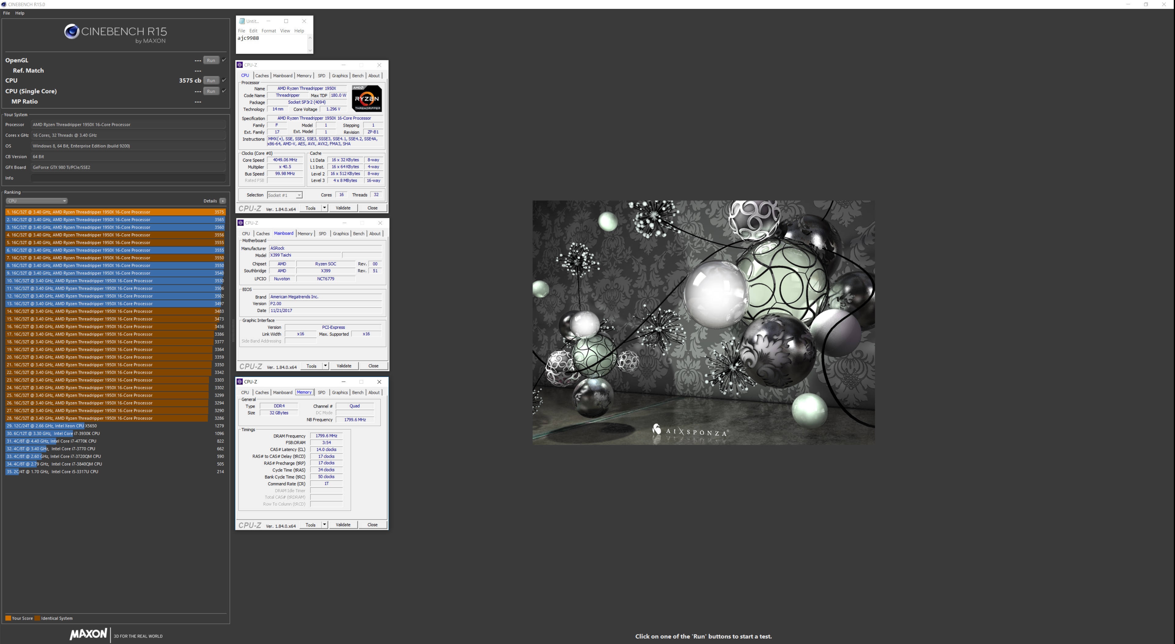
Got a score of 3575 in CB15 with that while at 4050MHz CPU and 3600MHZ on the ram at CL14 17 17Attached Files:
triturbo, jaybee83, hmscott and 1 other person like this. -
-
SenseMI -- What does it do for you on the new Ryzen 2000 cpus?
Level1Techs
Published on May 6, 2018
and what does it have to do with overclocking? how is overclocking different on these cpus?
ajc9988 likes this. -
Top 5 Best CPUs, Almost an AMD Ryzen Shutout! [May Desktop Picks]
Hardware Unboxed
Published on May 7, 2018
-
got it for msrp before the mining craze.
it allows for higher hbm2 clocks, but the core stays the same-ish.
The 1080 costs a bit more here, so it was a no-brainer to get the 56 and flash it to surpass the 1080.triturbo, hmscott, ajc9988 and 1 other person like this. -
It's a good thing you undervolted too.
I was wondering, how much did your power consumption improve from undervolting?
And for improving performance, you should likely just overclock the HBM to higher frequencies as the power draw on that is minimal vs core clock increases.triturbo, hmscott, jaug1337 and 1 other person like this.
AMD's Ryzen CPUs (Ryzen/TR/Epyc) & Vega/Polaris/Navi GPUs
Discussion in 'Hardware Components and Aftermarket Upgrades' started by Rage Set, Dec 14, 2016.