My PLL isn't supported by setfSB either but I can use it to overclock up to 333mhz fsb
there is a chipset feature that has to do with EIST which locks it at the 6x multiplier when its running on the wrong FSB.
Like MH said it will work with Nvidia chipsets
-
-
Could i maybe overclock my p7350 ? it has no EIST.
-
I think it does have EIST (enhanced Intel SpeedStep Technology):
Intel® Core?2 Duo Processor P7350 (3M Cache, 2.00 GHz, 1066 MHz FSB) with SPEC Code(s) SLB53, SLGE3 -
I got a Celeron t3000 DUAL CORE running at 2.4ghz with the 200>266mhz BSEL mod.
It will only boot in safe mode... I think I need more voltage.
What is the BSEL mod to increase voltage?
There is an example but no explanation, and its for socket M. Is it the same for socket P? -
You need to download the datasheet:
http://download.intel.com/design/mobile/datashts/32012001.pdf
Then just look at the VID table and the pinout. -
thanks, I did need that.
")
but I figured this one out. I don't know why it doesn't seem to boot to win7 64, but with XP 32 it runs well, stressed with ORTHOS and passed tests.
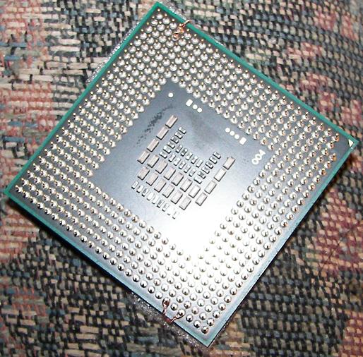
I think I increased voltage anyway. Here's a picture for anyone who may be interested:
![[IMG]](images/storyImages/58771d1290946046-bsel-mod-socket-p-explained-photos-z.jpg)
You should probably be able to orient yourself (if you are looking at a pinout unlike me) the top is 200>266 and the bottom is VSS connected to VID1.
I tried increasing my FSB to 333mhz, and I got a black screen immediately. Since I restarted it stuck at 2.9ghz 333mhz fsb and everything seems stable. link
And this a 1.8ghz Celeron I got for 25$ shipped
Attached Files:
-
-
Wow 333mhz worked?
I thought it wouldn't boot. I have to try this myself.
Can you run wprime on it?
I want to compare it with my SP9400.
I still wonder what is stopping CPUs with a 266mhz FSB from working with the old PM965 chipset. -
333mhz worked with setFSB. Is there a BSEL for 333mhz??
My laptop shutdown immediately when I overclocked to 1333mhz, then restarted still at 1333mhz totally stable. Maybe 1333mhz will adjust PLL frequencies automatically.
I haven't used WPRIME much, just checking it out. but at 2.4ghz it took about 38 seconds to complete 32m
I think the PM965>PM45 thing is about BIOS microcode. So maybe you can run any 800mhz FSB CPUs at 1066mhz in PM965, but EIST will probably still lock to 6x
I think I'll try this CPU in my PM965 laptop.
It will be really interesting to see what happens. Its an m1730, which no one has ever FSB overclocked and the PLL is unknown as of yet to even have a 266mhz mode. -
You should be able to BSEL mod it to 333mhz, but I have no idea if it will boot.
Look at Method 2 (FSLx+BSEL mod to hardwire PLL for higher FSB) here:
http://forum.notebookreview.com/har...pll-pinmod-overclocking-methods-examples.html
BSEL[2] -> high
BSEL[1] -> low
BSEL[0] -> low
Might give 333mhz. -
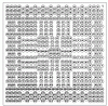
Congratulations on the great Celeron overclock. Would be interested in your PM965 results. I too believe it's microcode related. Worth noting that the PM965 chipset shuts down the PLL if it detects a BSEL other than 533, 667 or 800Mhz as shown below. ie: PLL is set to 133, 166 or 200Mhz respectively. Need to do a FSLx mod or use setfsb to overclock past 200Mhz.
![[IMG]](images/storyImages/pllfsb.png)
m1730 uses a CY28547 PLL as shown here. Would be a great one to add to the overclocked list. -
I don't understand why the BSEL would be necessary if I did FSLx...
I'm pretty cautious right now of soldering tiny things on my motherboard with a 60 watt. although someone else did it.
You only have to run a wire to ground pin45, not lift it correct?
Even with my limited soldering skills I have been considering doing that with my m1730 for a while. I do know how to not screw up horribly. My fear is entirely frying my PLL. -
So I connected BSEL2 to vcc, my notebook booted up fine but the FSB is still 266mhz (I was aiming for 333mhz).
Setfsb still shows FSLc as 0 (not 1, which I was looking for). -
Do you mean that if i do this on a CY28547 i will get 266mHz of FSB?
-
If you do the PLL mod then you should get 266Mhz. Would your T7300 work at 2.66Ghz is a different story.
-
Yes but i want to light mod the clockgen so i can reverse the mod somehow.
Can i pencil it or it won't be enough for the job? -
BUMP!
-
Might not be, I think if you don't cut the connection betwen the chipset and PLL, you will get the same result as a BSEL mod would give you (locked down to 6x multi).
-
I got to do it the hard way then.
Sh... wish me some good luck
-
Would this chipset be applicable to this mod? I'm interested (if I have the time in the near future).
Chipset model is: AMD M785 (RS880M) + Hudson-1 (SB810/SB850)
GPU is: ATI HD 5650
CPU is: AMD Phenom-II N930 -
I can't find the pinout for you CPU.
If you found the datasheet it would help a lot. -
Where does one start looking for the datasheet? Are there usual sites for it or is Google the only way?
-
Amd should have it on their website, maybe here:
Search Technical Documentation -
So for this to work, do I need the CPU datasheet or the socket datasheet?
-
No one knows. No one has ever done this for AMD. It could be totally impossible.
I think you need both but I'm not sure anyone here can really help you a lot with this.
This is the databook for your chipset http://support.amd.com/us/Embedded_TechDocs/47991.pdf
Heres what is all the way at the bottom:
And attached is a screenshot of the pinout diagram. Maybe this will get you started. I don't know a lot about what any of it means. I don't know if thats for the chipset BGA or actual CPU, either way its quite a change from intel...Code:Table A-1 RS785E Pin List Sorted by Ball Reference Ball Ref Pin Name A10 POWERGOOD A11 DAC_HSYNC A12 PLLVDD A13 VDDLTP18 A14 VDDLT33 A15 VDDLT18 A16 TXCLK_LN A17 TXOUT_U1P A18 TXOUT_U0N A19 TXOUT_L3P A2 VSSAPCIE A20 TXOUT_L2N A21 TXOUT_L1P A22 TXOUT_L0P A23 VDDHTRX A24 HT_RXCALN A25 VSSAHT A3 GFX_RX1P A4 GFX_TX1P A5 GFX_TX0P A6 VDDPCIE A7 DDC_DATA1/AUX1N A8 DDC_CLK0/AUX0P A9 I2C_DATA AA1 GPP_TX2N AA11 VDD_MEM AA12 MEM_A4 AA14 VSS AA15 MEM_DQ6 AA17 MEM_DQ5 AA18 MEM_DQ0 AA19 MEM_DQ2 AA2 GPP_TX2P AA20 MEM_DQ1 AA21 VDDHTTX AA22 HT_RXCLK1N AA24 HT_RXCAD10P AA25 HT_RXCAD10N AA4 VSSAPCIE AA5 SB_RX2P AA6 SB_RX2N AA7 SB_RX1P AA8 SB_RX0P AA9 VDDA18PCIE AB1 VSSAPCIE AB10 VDD_MEM AB11 VSS AB12 MEM_A0 AB13 MEM_CS# AB14 MEM_A6 AB15 VSS AB16 MEM_A5 AB17 VSS AB18 MEM_CKE AB19 VSS AB2 VSSAPCIE AB20 MEM_DQ12 AB21 VSS AB22 VDDHTTX AB23 HT_RXCLK1P AB24 HT_RXCAD9N AB25 HT_RXCAD9P AB3 GPP_TX1N AB4 GPP_TX1P AB5 VSSAPCIE AB6 SB_TX2P AB7 VSSAPCIE AB8 PCE_CALRN AB9 VDDA18PCIE AC1 GPP_TX0P AC10 VDD_MEM AC12 VSS AC14 MEM_A12 AC16 MEM_A10 AC18 MEM_DQ11 AC2 GPP_TX0N AC20 MEM_DQ8 AC22 MEM_DQ14 AC23 VDDHTTX AC24 HT_RXCAD8P AC25 HT_RXCAD8N AC3 VSSAPCIE AC4 VSSAPCIE AC6 SB_TX2N Ball Ref Pin Name AC8 PCE_CALRP AD1 GPP_RX2P AD10 VDD_MEM AD11 VDD18_MEM AD12 MEM_COMPN AD13 MEM_A8 AD14 MEM_A7 AD15 MEM_A9 AD16 MEM_BA0 AD17 MEM_BA2 AD18 MEM_WE# AD19 MEM_DQ9 AD2 GPP_RX2N AD20 MEM_DQS1P AD21 MEM_DQ15 AD22 MEM_DQ13 AD23 IOPLLVSS AD24 VDDHTTX AD25 VSSAHT AD3 GPP_RX1N AD4 GPP_RX0N AD5 SB_TX3P AD6 SB_TX1N AD7 SB_TX0P AD8 THERMALDIODE_N AD9 VDDA18PCIE AE1 VSSAPCIE AE10 VDD_MEM AE11 VDD18_MEM AE12 MEM_COMPP AE13 MEM_A11 AE14 VSS AE15 MEM_A3 AE16 MEM_A1 AE17 MEM_BA1 AE18 MEM_VREF AE19 MEM_DM1 AE2 GPP_RX1P AE20 VSS AE21 MEM_DQS1N AE22 MEM_DQ10 AE23 IOPLLVDD18 Ball Ref Pin NamePin Listings © 2010 Advanced Micro Devices, Inc. 47991 AMD RS785E Databook 1.30 Proprietary A-3 AE24 IOPLLVDD AE25 VDDHTTX AE3 GPP_RX0P AE4 VSSAPCIE AE5 SB_TX3N AE6 SB_TX1P AE7 SB_TX0N AE8 THERMALDIODE_P AE9 VDDA18PCIE B1 VSSAPCIE B10 STRP_DATA B11 DAC_VSYNC B12 PLLVSS B13 VSSLTP18 B14 VDDLT33 B15 VDDLT18 B16 TXCLK_LP B17 TXOUT_U1N B18 TXOUT_U0P B19 TXOUT_L3N B2 GFX_TX2N B20 TXOUT_L2P B21 TXOUT_L1N B22 TXOUT_L0N B23 VDDHTRX B24 HT_TXCALP B25 HT_TXCALN B3 GFX_RX1N B4 GFX_TX1N B5 GFX_TX0N B6 VDDPCIE B7 DDC_CLK1/AUX1P B8 DDC_DATA0/AUX0N B9 I2C_CLK C1 GFX_RX2N C10 LDTSTOP# C12 ALLOW_LDTSTOP C14 VSSLT C16 VSSLT C18 VSSLT C2 GFX_RX2P C20 VSSLT C22 VSSLT C23 HT_RXCALP Ball Ref Pin Name C24 HT_REFCLKN C25 HT_REFCLKP C3 GFX_TX2P C4 GFX_RX0N C6 VDDPCIE C8 AUX_CAL D1 GFX_TX3P D10 HPD D11 VSS D12 SUS_STAT# D13 TESTMODE D14 PLLVDD18 D15 VSSLT D16 TXCLK_UP D17 TXCLK_UN D18 TXOUT_U3P D19 TXOUT_U3N D2 GFX_TX3N D20 TXOUT_U2P D21 TXOUT_U2N D22 VDDHTRX D23 VSSAHT D24 HT_TXCAD0P D25 HT_TXCAD0N D3 VSSAPCIE D4 GFX_RX0P D5 VSSAPCIE D6 VDDPCIE D7 VDDA18PCIEPLL D8 SYSRESET# D9 TMDS_HPD E1 GFX_TX4N E11 REFCLK_P E12 AVDD E14 VSS E15 VSS E17 RESERVED E18 GREEN E19 BLUE E2 GFX_TX4P E20 VSSLT E21 VDDHTRX E22 VSSAHT E24 HT_TXCAD1P Ball Ref Pin Name E25 HT_TXCAD1N E4 VSSAPCIE E5 GFX_RX3P E6 VDDPCIE E7 VDDA18PCIEPLL E8 DAC_SDA E9 LVDS_DIGON F1 GFX_TX6P F11 REFCLK_N F12 AVDD F14 AVDDDI F15 RESERVED F17 RESERVED F18 GREEN# F19 BLUE# F2 GFX_TX6N F20 VDDHTRX F21 HT_TXCAD8P F22 HT_TXCAD3N F23 HT_TXCAD3P F24 HT_TXCAD2P F25 HT_TXCAD2N F3 GFX_TX5N F4 GFX_TX5P F5 GFX_RX3N F6 VDDPCIE F7 LVDS_BLON F8 DAC_SCL F9 VDD18 G1 VSSAPCIE G11 RESERVED G12 LVDS_ENA_BL G14 DAC_RSET G15 AVSSDI G17 RED# G18 RED G19 VDDHTRX G2 VSSAPCIE G20 HT_TXCAD9P G21 HT_TXCAD8N G22 VSSAHT G24 VSSAHT G25 VSSAHT G4 VSSAPCIE Ball Ref Pin Name47991 AMD RS785E Databook 1.30 © 2010 Advanced Micro Devices, Inc. A-4 Proprietary Pin Listings G5 GFX_RX4P G6 GFX_RX4N G7 VDDPCIE G8 VSS G9 VDD18 H1 GFX_TX8P H11 VDD33 H12 VDD33 H14 AVSSQ H15 AVDDQ H17 VDDA18HTPLL H18 VDDHTRX H19 VSSAHT H2 GFX_TX8N H20 VSSAHT H21 HT_TXCAD9N H22 HT_TXCAD4N H23 HT_TXCAD4P H24 HT_TXCLK0P H25 HT_TXCLK0N H3 GFX_TX7N H4 GFX_TX7P H5 GFX_RX5P H6 GFX_RX5N H7 VSSAPCIE H8 VDDPCIE H9 VDDA18PCIE J1 GFX_TX9N J10 VDDA18PCIE J11 VDDC J12 VSS J14 VDDC J15 VSS J16 VDDC J17 VDDHT J18 HT_TXCAD11P J19 HT_TXCAD12N J2 GFX_TX9P J20 HT_TXCAD10P J21 HT_TXCAD10N J22 VSSAHT J24 HT_TXCAD5N J25 HT_TXCAD5P J4 VSSAPCIE Ball Ref Pin Name J5 GFX_RX6N J6 GFX_RX6P J7 GFX_RX7P J8 GFX_RX7N J9 VDDPCIE K1 GFX_TX11P K10 VDDA18PCIE K11 VSS K12 VDDC K14 VSS K15 VDDC K16 VDDHT K17 HT_TXCAD11N K2 GFX_TX11N K22 HT_TXCAD7N K23 HT_TXCAD7P K24 HT_TXCAD6P K25 HT_TXCAD6N K3 GFX_TX10N K4 GFX_TX10P K9 VDDPCIE L1 VSSAPCIE L10 VDDA18PCIE L11 VDDC L12 VSS L14 VDDC L15 VSS L16 VDDHT L17 VSSAHT L18 HT_TXCAD13N L19 HT_TXCAD12P L2 VSSAPCIE L20 HT_TXCLK1N L21 HT_TXCLK1P L22 VSSAHT L24 VSSAHT L25 VSSAHT L4 VSSAPCIE L5 GFX_RX8P L6 GFX_RX8N L7 VSSAPCIE L8 GFX_RX9N L9 VDDPCIE M1 GFX_TX13P Ball Ref Pin Name M10 VDDA18PCIE M11 VSS M12 VDDC M13 VDDC M14 VSS M15 VDDC M16 VDDHT M17 VDDHTTX M18 HT_TXCAD15N M19 HT_TXCAD13P M2 GFX_TX13N M20 VSSAHT M21 HT_TXCAD14P M22 HT_RXCTL0P M23 HT_RXCTL0N M24 HT_TXCTL0P M25 HT_TXCTL0N M3 GFX_TX12N M4 GFX_TX12P M5 GFX_RX11N M6 VSSAPCIE M7 GFX_RX10N M8 GFX_RX9P M9 VDDPCIE N1 GFX_TX14N N12 VDDC N13 VSS N14 VDDC N2 GFX_TX14P N22 VSSAHT N24 HT_RXCAD7P N25 HT_RXCAD7N N4 VSSAPCIE P1 GFX_TX15P P10 VDDA18PCIE P11 VDDC P12 VSS P13 VDDC P14 VDDC P15 VSS P16 VDDHT P17 VDDHTTX P18 HT_TXCAD15P P19 HT_TXCTL1P Ball Ref Pin NamePin Listings © 2010 Advanced Micro Devices, Inc. 47991 AMD RS785E Databook 1.30 Proprietary A-5 P2 GFX_TX15N P20 VSSAHT P21 HT_TXCAD14N P22 HT_RXCAD5P P23 HT_RXCAD5N P24 HT_RXCAD6N P25 HT_RXCAD6P P3 GFX_RX14N P4 GFX_RX14P P5 GFX_RX11P P6 VSSAPCIE P7 GFX_RX10P P8 GFX_RX12N P9 VDDPCIE R1 VSSAPCIE R10 VDDA18PCIE R11 VSS R12 VDDC R14 VSS R15 VDDC R16 VDDHT R17 VDDHTTX R18 HT_TXCTL1N R19 VSSAHT R2 VSSAPCIE R20 HT_RXCTL1N R21 HT_RXCTL1P R22 VSSAHT R24 VSSAHT R25 VSSAHT R4 VSSAPCIE R5 GFX_RX13N R6 GFX_RX13P R7 VSSAPCIE R8 GFX_RX12P R9 VDDPCIE T1 GFX_REFCLKN T10 VDDA18PCIE T11 VDDC T12 VSS T14 VDDC T15 VDDC T16 VDDHT T17 VDDHTTX Ball Ref Pin Name T2 GFX_REFCLKP T22 HT_RXCLK0P T23 HT_RXCLK0N T24 HT_RXCAD4N T25 HT_RXCAD4P T3 GFX_RX15N T4 GFX_RX15P T9 VDDPCIE U1 GPP_REFCLKP U10 VDDA18PCIE U11 VSS U12 VDDC U14 VSS U15 VSS U16 VDDC U17 VDDHTTX U18 HT_RXCAD15N U19 HT_RXCAD15P U2 GPP_REFCLKN U20 HT_RXCAD14P U21 HT_RXCAD14N U22 VSSAHT U24 HT_RXCAD3P U25 HT_RXCAD3N U4 VSSAPCIE U5 GPP_RX4P U6 GPP_RX4N U7 GPP_RX5N U8 GPP_RX5P U9 VDDPCIE V1 GPP_TX5P V11 MEM_A2 V12 VSS V14 MEM_ODT V15 MEM_CKP V17 MEM_DQ4 V18 VDDHTTX V19 VSSAHT V2 GPP_TX5N V20 HT_RXCAD13N V21 HT_RXCAD13P V22 HT_RXCAD1P V23 HT_RXCAD1N V24 HT_RXCAD2N Ball Ref Pin Name V25 HT_RXCAD2P V3 GPPSB_REFCLKN V4 GPPSB_REFCLKP V5 GPP_RX3P V6 VSSAPCIE V7 VSSAPCIE V8 VSSAPCIE V9 VDDPCIE W1 VSSAPCIE W11 VSS W12 MEM_RAS# W14 MEM_CKN W15 VSS W17 MEM_DM0 W18 MEM_DQS0N W19 VDDHTTX W2 VSSAPCIE W20 HT_RXCAD12N W21 HT_RXCAD12P W22 VSSAHT W24 VSSAHT W25 VSSAHT W4 VSSAPCIE W5 SB_RX3P W6 GPP_RX3N W7 VSSAPCIE W8 VSSAPCIE W9 VDDA18PCIE Y1 GPP_TX3P Y11 VDD_MEM Y12 MEM_CAS# Y14 MEM_A13 Y15 MEM_DQ7 Y17 MEM_DQS0P Y18 VSS Y19 MEM_DQ3 Y2 GPP_TX3N Y20 VDDHTTX Y21 VSSAHT Y22 HT_RXCAD11P Y23 HT_RXCAD11N Y24 HT_RXCAD0N Y25 HT_RXCAD0P Y3 GPP_TX4N Ball Ref Pin Name47991 AMD RS785E Databook 1.30 © 2010 Advanced Micro Devices, Inc. A-6 Proprietary Pin Listings Y4 GPP_TX4P Y5 SB_RX3N Y6 VSSAPCIE Y7 SB_RX1N Y8 SB_RX0N Y9 VDDA18PCIE
Attached Files:
-
-
Bump!
I really have zero clue about what those mean, do any of this info relate to data on Intel CPUs? -
No. Thats what I'm saying. We can't help you.
Really, your guess is probably as good as mine. -
I have checked out the therad but one thing I do not understand is it says:
133 to 166 Mhz
133 to 200 Mhz
166 to 200 Mhz
BUT: my stock FSB is 267. So if I do the 133 to 200; my 267 stock FSB will increase with 67 Mhz (200-133=67) ? -
You can do 200>266, its just not listed on the first post. Heres how I did it:
So you should get a t9300 it will be 12.5 x 266 = 3.3ghz and then you can go on up from there
-
It will be 6x266=1.6Ghz if apply the BSEL mod with an Intel chipset. The Intel chipset compares the BSEL settings applied by the CPU and the ones samples by the chipset and if they differ you get a x6 lockout.
Need a FSLx PLL pinmod instead to get 266Mhz FSB with a T9300: http://forum.notebookreview.com/har...verclocking-methods-examples.html#post4998927 -
tuηay has nvidia mcp79d/730i chipset
-
I allready have my CPU at 267Mhz..
-
Yes... thats why you could overclock more with a cpu made for 200mhz...
-
Any risk to blast my MB and CPU away from my desk? I guess it is so?
-
lol I dunno... not until you find a way to increase up to desktop CPU voltages, at least.
I'm going to try that with a t1500 celeron dual core a 200% overclock cause its supposed to be 13 x 133 = 1.73 but it will be 13 x 266 =3.45ghz LOL
No i think going from 2.5 to 3ghz or a little more is not a big deal for the chips or motherboard... only a lot of overvolting would really burn something up -
Okay, if I got it right. If I do the same you posted on picture I'll get a increase of 66Mhz? Which will give me a FSB of 333Mhz.
But what do you think this cross to my therad? Will still my modules be a problem? -
No, I got the 66mhz increase to 333 later with FSB overclocking.
only the first 66mhz to 266 is gained by the pinmod. So you can't do it with your t9600, exactly like you said, its already at 266. -
Okey, so what can I do with my T9600?
-
Only the FSB overclocking
sorry.
There may be a way to bsel mod it to 333mhz, but that really would be no different than the other way except you dont have to deal with the RAM.
you should just try flashing your RAM. The latest version that can flash is 6.3.0.1 -
Okay, I'll try that tomorrow and post result in my therad.
-
I've tried with a T1400. I tried to go from 133 to 200 FSB (i.e. 1.73 to 2.6Ghz) but I failed. You might have to up the voltage to make the T1500 overclock to 3.45Ghz.
I've added a few diagrams to the first post to show the following pin mods:
133 to 266
166 to 266
200 to 266 -
This does work with a PM45 chipset right?
Since i have an E8435 with 1.2375 which is 100% stable at 1.1375 i'm very tempted to apply this mod and just uninstall all the undervolt software. -
A VID mod will work for you.
Here is the datasheet you need:
http://download.intel.com/design/mobile/datashts/32012001.pdf
VID table page 23.
From a quick look, seems you need to connect VID3 to Vcc. -
You have to know that not all voltages goes down after mod.
Only part of it is affected, which one? you have to read from datasheet. -
Okay going to do a mod, Considering that the GL960 is a socket P But the processor on my laptop is a celeron M 530 socket M 479mpga (But works cause it has 478 pins) I guess it is called socket M but is a socket P processor cause of the 478 pins instead of 479 pins.
What mod do I do? A socket M or P? -
I'm pretty sure the pinout is very different when you compare socket P to socket M.
Anyway I would go off of the chipset, so in your case I would do the mod for socket P.
There were two similar CPUs, Celeron M 530 and Celeron 530, the Celeron 530 is socket P. -
The pin out for the the BSEL/ FSB mod is actually the same. The VID pins are different though
-
Hello
I just started with pinmods, and have some issues...
From the beginning
Have:
*Extensa 5620z socket P
*PDC T2330 1,6 GHz
*PDC T2310 1,46 GHz
T2330 - Vid3(-Vcc) mod - passed
T2310 - Vid3 mod - passed
T2310 - Vid4 mod - at first short circuit, after little isolation passed
T2330 - Vid4 mod - BIOS passed - Win almost passed - after 2 min freeze (with or without RMclock)
T2330 - Vid5 mod - Only BIOS
T2310 - Vid5 mod - Passed? surprisingly via ClockGenie and Throttlestop run 0.9500 even on 1,46Ghz (11x133) in real it should be 0,6....
My worries - I aint found any big difference in heat so i think that due shortcircut i messed something with that T2310, or my shortcut wire is to thin (about 2/3 of pin thickness)
PS. Another mystery.... Without mods - in OCCT etc various processors from T2310 to T7250 un only 87-93% with mods 97-100% so its hard to check heat before-after :/ -
I have a T2310 myself and without pin mod it is stable @ 11x 133 with 0.95v. With orthos I don't have a problem. CPU load is 100% with or without pin mod. If you're laptop doesn't use an intel chipset you should try the BSEL mod. My T2310 is stable @ 2.2 Ghz (FSB 133 to 200) (chipset SIS though).
If the mod is successful you should see a different in temperature. Also note that some of the VID in RMclock (or similar program) will drop after the mod but not all of them. Check this post out for an example:
here -
Hello,
I have MSI GT628. I was successful with undervolting of C2D T6600 - that was easy mod, only one wire + settings in RM Clock and it was running on 0,925 V rockstable (power consumption about ~11 W lower).
But C2Q Q9000 seems to be harder and I would like to ask for some help...
The main problem is, that I don't know possible VIDs for this CPU - each program says anything else. With help of old RM Clock I determined, that the difference is made by settings "desktop × mobile CPU".
So:
RM Clock, forced@desktop = 1,1625~1,375 V
RM Clock, forced@mobile = 1,050~1,2625 V
CrystalCPUID = desktop = 1,1625~1,375 V
ThrottleStop = mobile = 1,050~1,2625 V
old CPU-Z = desktop
new CPU-Z = mobile
old Everest Ultimate = desktop
new AIDA64 = mobile
When I set e.g. 1,1625 V in CrystalCPUID, new CPU-Z shows VID 1,050 V, AIDA64 also, old CPU-Z shows 1,1625 V... So I'm confused and I don't know, which VID is the correct and for which VID have I prepare the mod...
I have tried:
-0,4, +0,2, +0,1 V; in CrystalCPUID set 1,1625 V ==> power consumption in full load was lower about 4 W, temperatures fell about 7°C (in comparison with default)
-0,4 V, +0,2 V; in CrystalCPUID set 1,1625 V ==> no change in comparison with line above
-0,4 V, +0,2 V; in CrystalCPUID set 1,1188~1,2 V ==> power consumption increased ~10 W (in comparison with default)
-0,4, +0,2 V; in ThrottleStop set 1,1625 V ==> power consumption in full load was lower about 10 W, difference in temperatures was about 8°C (in comparison with default)
I hope that I can go lower and lower, because voltage about 1,1 V is for 45nm CPU@2,6+ GHz...
My target no.1 is pushing the idle power consumption and temperatures as low as possible because of fan noise...
Sumarized:
How can I measure the real Vcore/which program shows the true VID?
=> detect, which VID would be better for pinmod => do the pinmod
Thanks for any help (and sorry about my English).
Regards,
JK
-------
P.S.:
Tip for all undervolters - you can measure the power consumption of whole laptop when you are running on batteries - use ThrottleStop, AIDA64 or similiar program, which can read from chip, which is placed on battery. Based on decrease of battery's cappacity is count actual power consumption - 100% accurately. And IMHO it's better way to detect functionality of the voltmod, than hocus-pocus with temperatures. ;-) -
RMclock with desktop setting doesn't give you the right reading
I know that RMclock reading is quite accurate, and since it is the same as ThrottleStop then you max Vcore is 1.2625v and min is 1.0500v.
Can you please explaining your aim from the mod. Are you trying to turn the q9000 into a ULV? or are you interested in overclocking you CPU to the limit?
can you tell me what is you min VID to run the q9000 stable @ 2GHz.
By the way how did you manage 2.6GHz? Software overclock? PLL mod?
BSEL Mod on a socket P explained with photos
Discussion in 'Hardware Components and Aftermarket Upgrades' started by naton, Jun 16, 2009.