I successfully overclock / overvolt/ undervolt my Lenovo T61 without soldering/cracking motherboard. Below is the short report.
Overclock:
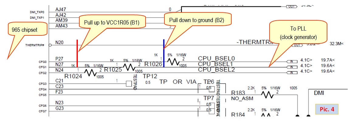
Problem: Intel chipset lock the CPU at lowest multiplier (6x) if it is forced to work at frequency higher than designed. In the case of 965 chipset the limit is 800MHz. For IBM / Lenovo laptops, the BIOS also prevents the computer to boot up.
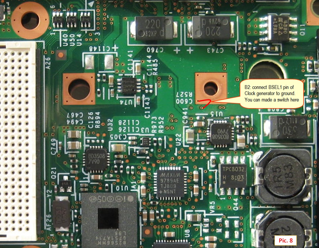
Research: The chipset determines working frequency using BSEL pins (CFG0-CFG2 on Picture 4 for 965 chipset). Fortunately, for Lenovo T61 there are three 1K resistor between BSEL pins of the chipset and BSEL pins of the clock generator (Resistors 1024-1026 on Picture 4). Therefore, we can cheat the chipset by putting different voltages to it’s BSEL and clock generator BSEL pins.
Solution: Pull-up BSEL pin of the Chipset to VCC line and pull-down BSEL pin of the Clock generator to ground. For overclocking FSB from 200Mhz to 266Mhz, we need to mod BSEL1 (see Picture 4).
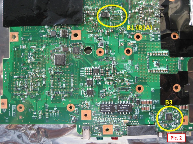
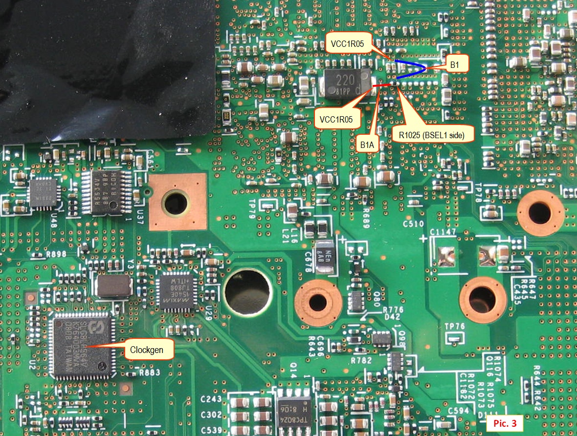
Practice: On Picture 3 the B1 pinmod was made to pull-up BSEL1 pin of the Chipset to VCC1R05. Connection was made by ATA-66 cable to the two holes on the motherboard (in order to keep warranty). Later, if the overclock is successful, you can (permanently) solder B1A mod between R1025 resistor and near by big capacitor.
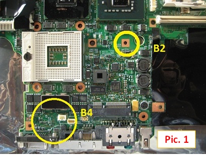
On Picture 8 the B2 pinmod was made to pull-down BSEL1 pin of the Clock generator to the Ground (there is a line connected the hole on Pic. 8 to pin 7 (BSEL1) of the clock generator). For switchable overclock, you can make a switch here (I keep the switch in the unused modem jack).
Extra: The IDA problem. When IDA is activated, the Penryn CPU gets very high multiplier /frequency, e.g. 14x/3.724Ghz @ 266Mhz FSB for T9500 CPU. To make overclock stable, you need to disable IDA. Following advice of one Chinese guy on 51nb forum, I disabled Speed Step in BIOS (Config -> Power Option -> Intel Enhanced Speed Step -> Disable). However, in my observation, this not fully disables Speed step, because in Windows 7 my overclocked T9300 (at 3.2Ghz) falled in Prime Blend Test after 10-15 min during transition between test modes, for example between 1024K and 8K, while it is rock stable in Prime Small FFT test (harder for CPU/FPU). The Min and Max CPU are set to 100% in Power profile of Windows 7. The problem is less frequent on Windows XP.
--------------------------
Overvolt:
Problem: A regular method is to connect some VID pins of CPU to VSS pin, for example VID2 to VSS to overvolt by 0.05v. However, this can disable some voltage in the VID table, what is not good for me because I also want to undervolt by moding VID4 (see below).
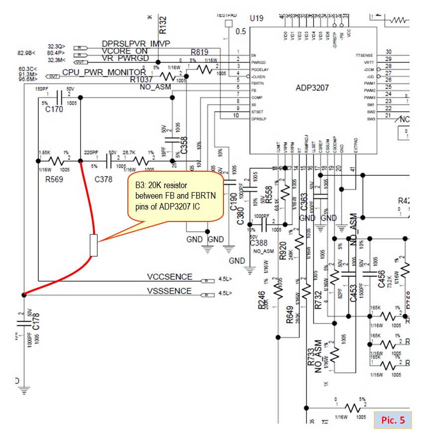
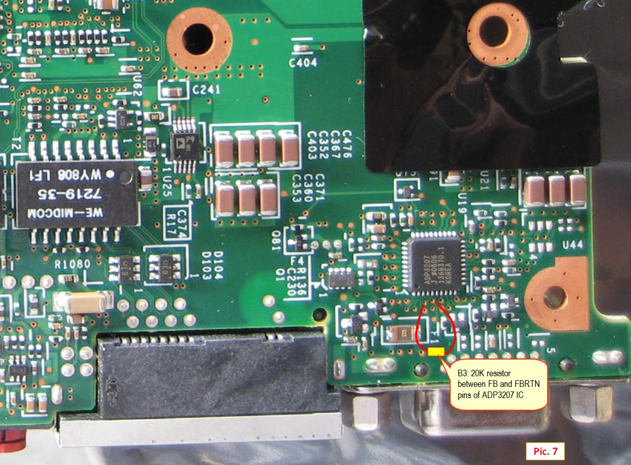
Research: In the feedback circuit of VCC_CPU_Core regulator ADP3207 IC (Picture 5) there is a 1.65K R569 resistor. We can design a simple voltage divider here.
Solution: Put a 20K resistor between right side of R569 and VSS_SENSE line. Thus, we make a 92% voltage divider before VCC_SENSE go to Feedback pin of ADP3207. The voltage will increase by 8% for all values in the VID voltage table.
Practice: See B4 mod on Picture 7. It is very important to make reliable contact to the holes (I used a acurately filed leg of a 0.5W resistor for this purpose).
-------------
Undervolt:
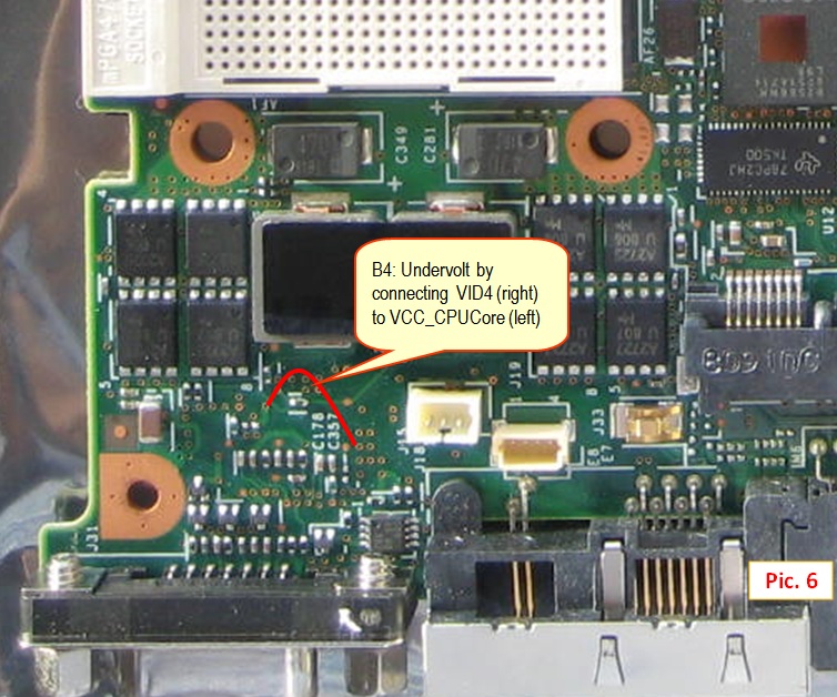
Problem: You can use VID to VCC mod (in my case VID4 to VCC mod to undervolt by 0.2v, from lowest 0.925v to 0.725v). However, for Core Duo CPU the VCC pins are located far from VID pins -> not easy to make mod, unlike VID to VSS mod. Moreover, when make VID4 to VCC mod, the computer may hang up because in low power states it requires a voltage somewhere between 0.5 and 0.7v, and due to the mod, the voltage can be as low as 0.3-0.5v.
Solution: Use external holes on motherboard to make the mod. In parallel, make a overvolt as described above.
Practice: see mod B4 on Picture 6.
-----------------
Results:
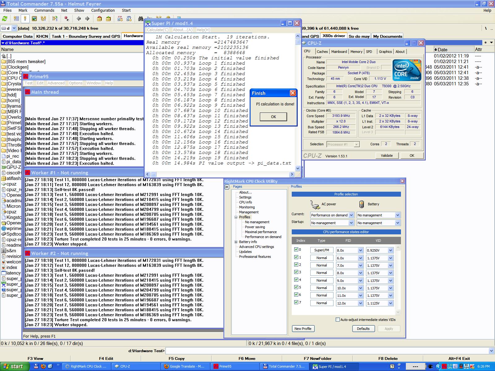
T9300 overclocked to [email protected]. Do SuperPI 1M less than 15 sec. See attached picture. Temperature in Prime Small FFT is about 82-85 deg (ambient temperature 18 deg Celsius).
However, as it was described above, the T9300 is not very stable with Prime Blend Test (due to IDA ?), so I have to make VID2 to VSS mod to force it to run at 1.375v (with 8% overvolt) in IDA mode and 1.27v at 3.2Ghz (because after mod, the voltages between 1.20 and 1.27v are not available). Too hot for me. So I replaced it by a T8300, and it is fully stable at 1.20v.
Therefore, my current system is:
Lenovo T61 frankenpad in T60p UXGA IPS chasis, [email protected]@1.20v, undervolted by VID4 to VSS mod and overvolted by 8% by feedback circuit mod. At lowest multiplier (1.6Ghz), it works at 0.775v!
-------------
PS. Pic1 and Pic2 is overview of mods.
The forum allows only 6 attachment. So see the rest of pictures in the next post.
-
T61 OC: The rest of pictures.
Attached Files:
-
-
^ what a wonderful work from Binh
 ... first to manage to OC the T61 by increasing the bus speed while tricking the chipset, hehe.
for OC purposes you'd be better off disabling IDA from the BIOS, as it requires much bigger voltage step increase (~5x times) than what it is needed between regular multipliers. Thus at high frequency the chip would heat up by a lot more.
---
I would like to add the performance increase note here, as I've calculated it based on the CPU performance charts from here:
PassMark CPU Benchmarks - High Mid Range CPU's
T8300 - stock score 1,489 => OC to 3.2GHz is 33.33% increase => estimated score 1,985
T9500 - stock score 1,839 => Dual IDA to 2.8GHz is 7.7% increase => estimated score 1,980
X9000 at 3.2 GHz smokes both obviously at estimated score of 2,262, which is 23% over stock T9500, with the expected temperature increase over both of the above of course, thus would be the practical limit for performance enthusiasts. Temperatures could go above 90 deg C here so watch out.
- note 3.2Ghz clock requires about 1.2 Volts to operate. T8300 having 3Mb of cache would not heat up as much as X9000 (no IDA) with its 6Mb cache at the same speed and voltage. It seems that T8300 at 3.2GHz at ~1.2V would heat a little over T9500 at Dial IDA at 2.8GHz at below 1.1V while producing the same performance. My T9500 at Dual IDA at 1.0750V is stable and tops at about 80 deg C with TPFanControl running the laptop fan at max speed (the 64 setting).
- now go and try X9100 with E stepping using the same chipset tricking method, as it would have lower temperatures compared to the X9000 so higher speeds could be very well managed
EDIT: if you'd like to further improve the cooling abilities of the T61, if you have space (just like I have on my 14" standard screen but not on my 14" wide screen T61) then you can drill holes on the plastic bezel just above the fan assembly, which would make the suction air flow cooler due to not having to go through the laptop internals first. Laptop would not look stock anymore of course. Taking off the keyboard produces the same effect, but I'm guessing that would not be permanent solution, hehe. -
Great find, but still 2 much for me ~~. When i had my T61, I had once used it for 3 month with keyboard lift off cause the fan is semi dead. I had the keyboard attach to cable but slanted resting on the speaker.
-
Hi everyone.
I'm using a Studio XPS 1645 laptop, which has also SLG8SP585V as PLL like XPS 1647 and Acer Aspire 5740G, its chipset is PM55 (Intel(R) 5 Series/3400 Series Chipset Family SMBus Controller - 3B30), Super IO chip is IT8512E per RW.
I tried to change BCLK with latest version of SetPLL and LUT files provided by courtesy of MotoVlad for SLG8SP585 of his Aspire 5740G (2 versions: with or without Pinmod found in his post in acerfans.ru), but it didn't work on my PC.
Here are some error messages I got when trying to use SetPLL and RW
setpll -read ---> "SMBus Error"
setpll slg8sp585 135 ---> "Failed to set BCLK"
Click on "Clock Generator" in RW ---> "SMBus return error, clock generator may stop response"
Click on "SMBus Device" in RW ---> Nothing appears in new window.
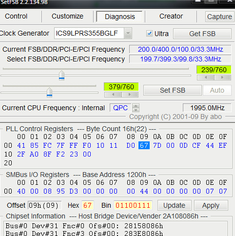
In SetFSB Diagnosis Tab, I got nothing on "PLL Control Registers", and here is what displays in "SMBus I/O Registers" and "Chipset information":
SMBus I/O Registers ---Base Address 1840h---
00 01 02 03 04 05 06 07 08 09 0A 0B 0C 0D 0E 0F
00 44 00 14 00 D3 08 00 00 00 44 00 00 14 00 07 07
Chipset Information ---Host Bridge Device/Vendor D1328086h---
Bus#0 Dev#31 Fnc#0 0fs#00: 3B038086h
Bus#0 Dev#31 Fnc#3 0fs#00: 3B308086h
What information should I have (motherboard version, proper SMBus setting, etc.) to get a LUT file which work with my PC? How can I create a working LUT file?
Thanks in advance -
Good work. You can check the 'disable Turbo' option in Throttlestop to fully disable IDA mode. Then your T9300 will run OK.
Dell wire their SLG* PLL's SMBUS lines to a MEC* controller
I had the same PLL in a Dell E4310 with the same errors you describe above. Kizwan also with the same PLL in his Studio 1557 too with the same errors.
Turns out that Dell wire the PLL's SMBUS lines to an EC controller, (SMSC MEC5045) rather than to the Intel IBEX Peak chipset. Dell have set that MEC controller to hide the PLL. So no amount of using setpll/r-w/setfsb/i2cdump can get the PLL info. What's worse is there are no public datasheets on the SMSC MEC* controllers so we could potentially 'unhide' the PLL.
As you have an i-core CPU, the PLL supplied can only be pinmodded to run at 100/133Mhz, with 133Mhz being the default. So only way of getting an overclock would be to disassemble the bios to reverse engineer the MEC* controller OR (not feasible) - rewire the PLL's SMBUS lines to the IBEX Peak controller.
I wish it wasn't so...triturbo likes this. -
Reverse engineer...
Thanks a lot for your quick response, it seems to be another dead end here. I kind of have seen that SMSC chip on a HP Envy 15, and will check on my PC to see this damned chip. -
Thank you for all your effort here, you did really good job.
I must say that I'm impressed and very willing to try this by myself.
The thing is - while I know about computer internals enough to do LCD/Mobo swaps, build PCs etc I know really little about electricity, soldering etc.
Basicly, what I've ever done is only soldering two wires and etc simple things.
Taking this into consideration, do you think that I could handle doing this mod by myself?
If yes, could you explain me please, step by step (pictures are welcomed), what I would need to do to get my T8100 @ 3.2 GHz @ 1.20v?
I'm young, brave man, who wants to learn new things
-
Hello guys. Is there any method to overclock MSI GX660 i5-460m CPU ? Can I use SetPLL, and if yes, which PLL should I use and what is the procedure ?
EDIT:
OK, so I have found that my PLL is ICS9LPRS113AKLF. So now I need to creat LUT file for SetPLL. I've did run a free version of SetFSB but I have got strange results comparing bytes. Most of people need to change two or three bytes, but in my example I need to change like 6 or even more bytes ( I am comparing SetFSB Diagnosis with 133MHz FSB and 139MHz FSB ). Strangely, when i change slider to 139MHz in SetFSB and click SET it is just going down to 45MHz and the clock does not change. Can anybody help me with this ? -
Hi guys,can someone help me pinmod my Vostro 1510 with a C2D T5670,Intel 965PM?
-
Vostro 1510 schematic tells us is has a ICS9LPRS387BKLFT PLL, same as a M11xR1 so you could do a TME-unlock as described in http://forum.notebookreview.com/ali...rther-overclock-m11x-r1-slg-hardmod-only.html , then do software overclocking up to the point of instability.
-
Hey nando4,according to http://forum.notebookreview.com/alienware-m11x/463095-m11x-clock-generator-ics9lprs387bklf-12.html, I don't need to do a pin-mod because in step 2),byte 09h,my hex is 25,and that bit which tells us whether overclocking is enabled is a 0,so overclocking is enabled,but whenever I try to change according to the last step(from 44 to something),when I click update and apply it doesn't change.I can't do step 4 either,and step 5,my hex is already 65.So do I need to do a pin-mod anyway?
-
I opened up my Vostro and took out the motherboard,it has an ICS 9LPRS365BLGF.Problem is,I don't know which pin to cut(which side) because it is different from the one in the picture of the M11x.1)Is the thing that says 14.318.
Attached Files:
-
-
Good that you opened up the system but that photo is terrible - I can't see anything at all. I'll take your word for it. That PLL would be the right vintage for the system. The m11xR1 PLL is newer and it didn't make sense why that same PLL would have been in your system.
You already checked byte 9 and confirmed TME was not locked. In which case use the freeware setfsb, select the ICS 9LPRS365BLGF PLL and see if it will overclock OK. If it does, then use Throttlestop to control the voltage and divider to identify the maximum stable overclock you can achieve within thermal limits. That's 100 degrees under full load, though I'd suggest going for 93 degrees max to give cooler running and a margin of safety. -
I already tried that,but it didn't work.When I click 'setFSB'it would have no effect.
-
BTW can someone tell me how to use SPDtool?
EDIT:Never mid,figured it out myself. -
original registers
![[IMG]](images/storyImages/originalb.jpg)
modded registers
![[IMG]](images/storyImages/moddeda.jpg)
this is what i tried without results:
1. hex E5 is bin 1(1)100101, (1) means pll is locked against overclocking
2. here i enable 22 registers instead of 13 (hex 16 is bin 22)
3. hex 61 is bin 01100(00)1 > i change to hex 67 which is bin 01100(11)1. i keep all the other bits except (00), so sata clock runs on pll2 and src on pll3
4. hex 01 is bin 0(00000)01 > i change to hex 65 which is bin 0(11001)01. i keep all the other bits except (00000), so i enable pll3 and pll2, disable src and pci divider, and enable cpu divider
5. i enable m/n divider by changing hex 00 to hex 01, which is bin 00000001
6. the problem is here, no matter the value i change in 0D or 0E that, after update and apply, it always change back itself to 49 and 4E. changing 0D and 0E has no effects, overclocking is not enabled? changing those bytes are not allowed by pll?
i tried changing hex 4E to 5E (that is hex +10), then update and apply, but setfsb shows 4E again
can someone help???
thanks -
Hello everyone.
My laptop is hp pavilion dv6-1220so and it's PLL is ICS 9LPRS355BKL. I managed to TME unlock it by cutting off the pin11 and pointing it to the GND via 10k resistor. As you can see register 9 bit 6 is 0 so it's worked.![[IMG]](images/storyImages/m2664mhz.png)
But the problem is when I'm pressing Set FSB button, my system is freezing, even if didn't changed FSB. I'm getting black screen with some vertical lines shuttering all the time. I don't know what to do, can somebody help with this? -
thanks a lot nando
im gonna cut pin 14 track
could someone take a picture of nav50 pll to see if pin 14 is attached to a resistor, so that removing resistor voids pin 14 without having to cut
this is only picture i found
![[IMG]](images/storyImages/ll2zv.jpg)
thanks
according to pll datasheet here, pin 14 is PCI2/TME, I/O type:
3.3V PCI clock output / Trusted Mode Enable(TME) Latched Input. This pin is sampled on power-up
as follows
0=Overclocking of CPU and SRC allowed
1=Overclocking of CPU and SRC NOT allowed
After being sampled on power-up, this pin becomes a 3.3V PCI Output
once booted, pin 14 becomes 3.3v pci output, does this means that it may affect pci features if i cut the track? is there any risk affecting laptop performance if i cut the track?
thanks -
how do i disable speedstep in bios and xp so that cpu always run at max speed (166x10=1660mhz)? how do i choose this behaviour only with ac power?
this is my nav50 1.26 bios with unlocked power menu
![[IMG]](images/storyImages/6852238075_78cb4b29b2_z.jpg)
thanks
here is full bios gallery
edit: disabling IST Configuration doesnt have any effects
but disabling C-States Support, which also disables 5 lines below, it works: cpu always running at 1660mhz -
hi, i have completely disassembled nav50, and know what?
pin 14 of pll is already disconnected, it lacks resistor, it leads to anything, i have checked continuity with multimeter, see pics. the track begins on one side of the mainboard, then continues on the other side to a lacking resistor.
so, why is setfsb showing that it is tme enabled (overclock disabled)? do i still need to connect pin 14 to ground? is not enough to be disconnected?
thanks


edit: i found out that pin 14 track end was connected to bat+ through the resistor above, so tme is still enabled -
i finally cut and connected pin 14 to gnd through 10k resistor
now tme is disabled but i dont know which 0D and 0E hex values to use, i tried the ones here but computer froze
also tried adding hex +10 to 0E but it also froze
can you help?
thanks -
-
I'm not able to set SRC to PLL3, but SRC to PLL2 works fine, what's the problem?
With Dufus' guide i'm able to change my FSB but i get BSOD after couple sec's. -
OK,I cut both pin 4 and pin 57,which should make TME-Disabled(although it already was according to setFSB) and set the FSB at 266Mhz,but I still can't overclock??It's still at 200Mhz(maybe luckily),but when I press setFSB,nothing happens.Have I done something wrong?
-
pll is running at 166mhz base frequency
this is what i got up to now: 166 >170 = 1663mhz > 1705mhz
these are the values working:
fsb, 0D, 0E:
-----------
166.3, 49, 4e
168.4, 49, 4f
170.5, 49, 50
then if i set 0E as 51 the laptop freeze/reboots/black screen
so 0D must change from 49 to other hex value, i.e. 48
any idea?
![[IMG]](images/storyImages/13395735.jpg)
![[IMG]](images/storyImages/56316084.jpg)
it both works with speedstep enabled (two speeds) or disabled (always max speed)
im afraid so many trials may destroy pc or hdd, im gonna try to make the tests with hiren's mini xp booted from pendrive (on-the-fly), without hdd
edit: i forgot saying that if i restart computer, it freezes, i must shutdown -
I have been looking into overclocking the cpu on my acer aspire 6920g. When I try to overclock with setfsb my and click 'set fsb' It always jumps back to normal.
my chipset is the intel 960 with the ics9lprs365bglf PLL.
If a pin mod is needed I'm sure I can do that, just need to know which pin to ground!
Thanks in advance. -
do you know someone who successfully pinmodded fsb 166 > 200 in acer nav50 with ics9lprs387bklf pll by cutting fsla pin 20 and connecting it to ground through 10k resistor? pin 20 is both fsla and usb_48mhz clock output 3.3v, will usb port be disabled?
thanks
![[IMG]](images/storyImages/fsla.jpg)
-
Hello again so, I managed to get modded bios so now I am running my P8400 on dual IDA 2400mhz 1.0625V. Finally I thing I get right MB datasheet. since there is no exact same with ATI and DDR3 this one seems to be closest I will ever get.
Image-Share - image-jpg-1408-192
So figure what side of resistor I should isolate and connect to GND, right ?
same picture of SLG..513v in higher resolution
Image-Share - image-jpg-1322-252
so my question is am I right ?
-
Is there anyone to help me clear about my pll ???
My system is MSI CR420 (i3-380m cpu, 2526MHz, BCLK=133, multiplier=19).
‘cause I'd wanna overclock my system, I disassembled my laptop to identify the PLL.
It was marked with “ ICS RS3199AL …. ….”
So, I ‘ve been searching for the data of “RS3199AL” with google help .
But, nothing ‘s yet…
If anyone know about that pll, RS3199AL, please let me know about it, too.
-
hi, i want to do FSLx pinmod in acer nav50 with pll ics9lprs387bklf
i would like moral hazard, nando4, davygt, dufus etc to give me an answer:
what if i cut pin20? is it safe? will it affect usb bus? please see pics:
ICS PLL:
![[IMG]](images/storyImages/17916150.jpg)
Intel Platform Controller Hub NM10
![[IMG]](images/storyImages/33047720.jpg)
MODIFICATIONS
![[IMG]](images/storyImages/68320437.jpg)
manufacture date of my laptop is march 2010, so modification 09/03 is implemented, and what is T64 at the end of pin 20 bus?
full schematics: http://lqv77.com/download/849/
please help -
I think it will affect the usb bus and the notebook will not POST.
But that's just my guess. -
thanks moral hazard for your answer
so there is no way to set FSLA as 0? i think i remember a russian forum where someome managed to set a 0 at boot by means of zener diode or something like that without disabling that pin...
the fact is that i donated SetFSB but abo and me didnt manage to make my pll work beyond 172.4 mhz (stock bus is 166mhz) so we gave up
maybe hex values are wrong, or ram is poor (kingston ??) or pcie bus must be raised, it must be a problem of sata bus -
If i remember correct, that pll chips has 2-3 lines with numbers and letters
For example:
ICS ab1cd2...
xy1xy2xy3xy4...
Probably you took the first line as your pll. Take a look again -
hey guys,
i have the ICS 9LPRS355BGLF PLL.
While using setFSB i can't hit setfsb- i move the first bar and when i hit setfsb the cursor goes when it was in the first place.
Take a look at the diagnosis screenshot.Attached Files:
-
-
Well, it seems that u have TME mode enabled, so you cant change FSB, unless u pinmod your motherboard.
-
thanx for the reply.
i disassembled again my lappy & captured the image to follow your advice.
so... attached the picture here..
-
maybe that ic is not a pll, 32 pin only? for example, my pll has 72pin
look for bigger ic named ics..., rt... or slg... -
Looks like the same sort of PLL as uses in an Acer 3820TG (ICS V3197BL). Those PLLs have only a 100Mhz and 133Mhz pin setting, so no pinmod is possible. The Acer PLL does allow software overclocking using setfsb when you select the 'ASUS G73JH' PLL so perhaps that is worth a go?
-
there is no another "ics ... "
-
I think it is the pll, it is one used for the newer hm55 chipset.
But because it is so new, you won't find the data sheet unless you email idt.
Or look at a similar pll on the idt website. -
oh ! thanx a lot, nando4.
it's a good information to me.
now i'm gonna try it.
btw, what is the name of PLL for "ASUS G73JH" ??? -
thank you for your interest.
but, what is it, 'idt' ?
-
idt is the pll manufacturer
IDT - Integrated Device Technology
go support > technical support > and ask for datasheet -
does anyone understand this mod?
![[IMG]](images/storyImages/175318.png)
![[IMG]](images/storyImages/175319.png)
![[IMG]](images/storyImages/175320.jpg)
thanks -
thanx a lot, manocao.
i'm digging in my laptop overclocking.
pls.. god take care of me..! -
This is a overclock of santa rosa based Fujitsu Siemens U9200
On the first picture, the 10KOm resistor is modded by grounding one of its leg. Therefore, the 4th leg (BSEL1?) of PLL is changed from 1 to 0 level.
You can use google translator to translate original article from Russian to English.
If you have problem with some Russian words, let me know. -
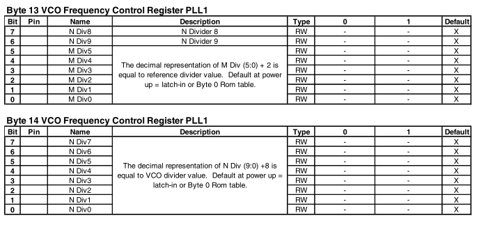
how does m-n divider work? which is the formula if i wanna get i.e. 166mhz fsb? i mean, is there a formula of this kind i.e. m/n=fsb?
in my case, at 166 mhz fsb, hex value for byte13 is 49, and byte14 is 4E, so m=11 and n=598, which is the formula that relates these 3 variables?
![[IMG]](images/storyImages/77398d1334418761-pll-pinmod-overclocking-methods-examples-m-n-divider.jpg)
Attached Files:
-
-
Well,can somebody explain this method cause i messed up in my mind
Thanks -
So guy's, as i posted before i managed to TME-unlock my laptop with ICS 9LPRS355BKL, but i still have problems with overclocking it. When What do i do wrong? Could the ''Gods'' of this thread help me?
PLL Pinmod Overclocking Methods and Examples
Discussion in 'Hardware Components and Aftermarket Upgrades' started by moral hazard, Jun 24, 2009.