
Wait so does this mean that we won't see Kepler mobile till Q3 or is this being read completely out of context?
-
nvm kepler talk is bs.
-
That was very interesting that you checked the aida release notes!
There is some more info! The Geforce 640 is also a gf116 rebadge such as the 620m..
Now where is our 650m ? I really want to know if its a rebadge ! -
It is GT640 other than GT640M.
GT640M may be a trimmed down GK107, at least I hope.
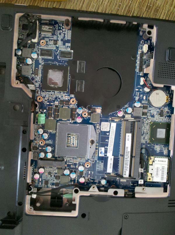
BTW:We have 650M chip pic in W110ER thread. And it does look like a new chip other than a rebadged one. -
yes but why should they rebadge higher GPU's like the 670m and 675m and produce them in 40nm and then make a 28nm 650m chip? This would be the only (early) kepler chip then, doesnt really make sense? I think the kepler yields are so bad that they will use all the 28nm capabilities for the desktop cards and release the real kepler mobile chips later
And I know of the picture, but I cant tell if its 28nm or can you? Maybe the chip looks different but the 555m also made several transitions (gf106 to gf116, also a new chip but nearly the same perf; Now the 555m is even called GF116M if you follow aida releasenotes)
The 650m is probably a rebadged 550m with a higher clockspeed, everything else wouldnt really make sense or? But I still think its very impressive for an 11 inch to have a 550m rebadge -
GT540M/GT550M have been rebadged as GT630M.
While GT555M has been rebadged as GT635M.
It would be ridiculous that nvidia made GT650M weaker than GT635M. -
only 540m was rebadged as the 630m, atleast till now there is no 550m rebrand out there
I think its ridicilous that nvidia rebrands the 40nm at all especially the high end ones.. -
Two pics for comparison.
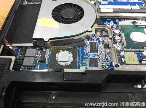
One is GT650M on W110ER
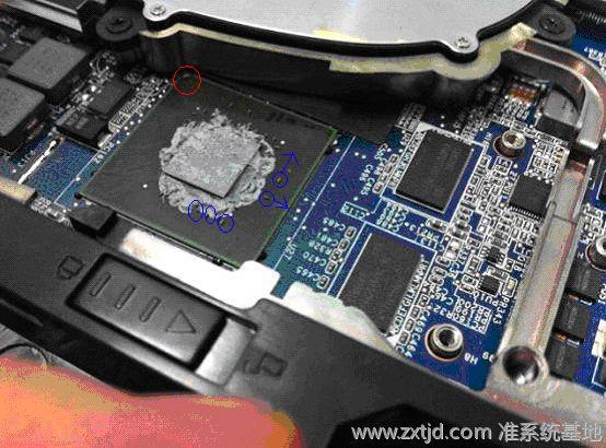
Another is GT555M(GT635M) on W150HRM![[IMG]](images/storyImages/75913d1330167657-semi-accurate-speculative-pricing-details-p150em-gt650m.jpg)
GT650M has a smaller die than GT635M.![[IMG]](images/storyImages/75912d1330167657-semi-accurate-speculative-pricing-details-p150em-gt555m.jpg)
Smaller size and higher performance imply a 28nm chip.Attached Files:
-
-
One second, you are comparing the Enthusiast Class 555m (or 635m) with the 550m
The 550m though is similiar to the 540m chip, which looks like the chip in the 11.6 inch clevo picture you posted
Here is a picture of the 540m chip (which the 550m is based on) which looks like a similiar size to the 650m
Here is even a picture of the 550m from the y570 mainboard (the chip on the top of the picture)
![[IMG]](images/storyImages/n5hu36.jpg)
And here the clevo 11.6 inch from your picture
As you see the smaller die size doesnt really tell us if its 28nm, since the 40nm 540m and 550m have the same die size as the 650m in the 11 inch clevo..
Im not trying to argue, believe me I wish that the 650m is stronger than the 555m because I really like compact notebooks with optimus and relatively strong GPU power -
Performance:
550M < GT555M=GT635M < GT650M
So GT650M is not a rebadged GT550M. -
Lets hope so! I still dont think its a 28nm part.. If nvidia really rebrands the 570m and 580m
The naming isnt a good indication though, especially with nvidia, there are often times cards with higher numbers which have slower perfomance, their naming is messed up
-
GT650M
![[IMG]](images/storyImages/75914d1330169235-semi-accurate-speculative-pricing-details-p150em-gt650m_another.jpg)
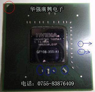
GF108(GT425M/GT435M/GT525M/GT540M/GT550M)
![[IMG]](images/storyImages/75915d1330169235-semi-accurate-speculative-pricing-details-p150em-gf108.jpg)
You may check their difference.Attached Files:
-
-
what does that proof? as I said there are many revisions of the 555m for example and many variations..
especially moving from the gf106 to gf116 the 555m chip had some changes... So the 650m chip will probably also look different than the 550m
Im not saying the 650m is completely the same chip, but It will probably not be significantly more powerful than the 550m if the 670m is only about 5 - 10 Percent faster than the 570m
And as you see in the pictures the die size looks nearly the same -
Yep nearly, but they aren't laid up next to each other so it's hard to tell by eye

-
It is not a 540m chip but MCP79MXT-B2 with GeForce 9400M integrated.
-
yes but the other chip is from the y570 mainboard and from your picture too
so whats your point? the die size from the 650m to the 550m isnt different as you originally claimed as you can see in these pictures
-
What I claimed is 650m and 55 5m have different die sizes while GT650M has higher performance than GT555m and of coz GT550M.
Many chips have similar die size as GF108(e.g. G96B). Does it mean GF108 a rebadge of G96B? -
you were the one that mentioned different die sizes as an explanation for the 650m being kepler, remember?
Its kind of obvious the 650m and 555m have different die sizes, since the 650m is the followup of the 550m and belongs to another perfomance class then the 555m which belongs to the enthusiast class.. So why do you compare two chips which are different in the first place ^^
So if you compare the 650m, then compare it to its predecessor the 550m (which look about the same size)^^ -
Then how can you prove 650M a rebadged 550m?
How can you explain an over-class performance increase? -
Ask nvidia how they come up with such crappy naming schemes haha
Lets just wait and see, if were lucky we will get some definite answers when the Cebit in Germany starts (Maybe im going there since I live in Germany) on the 6th of March.. Its rumoured that all the notebookvendors display their new IVB products there
I thought about taking my USB Stick with me, with some benchmark programms and hwinfo apps like gpu-z and so on and just get some real numbers from the notebooks shown there (IF they are shown there) -
You are sailing on the unknown sea of nothing.
Source: http://forum.notebookreview.com/sager-clevo/647054-clevo-w110er-ultraportable-4.html#post8338348
And the 650 isn't even close to being a 555m rebrand.. just sayin -
You all should have learned long ago, that those performance slides AMD and Nvidia release are mostly misleading propaganda.
For one, we don't even know which GT 555M they were comparing to this mysterious 650M. It could've been the weakest one they could produce. I'll bet anything that they didn't use the 144 core w/ 192-bit DDR3 or 128-bit GDDR5 versions.
The 650M is not looking like it has the specs to beat either one of them. -
-
No, that's a different generation of cards, you can't compare a 295 to a 405, how else are they going to push out refreshes of cards if they don't go up in number? If you're stupid, okay, that's one thing. But we're talking SAME generation, please show me a case where a lower numbered card is faster than a higher numbered card, SAME generation, not different generations.
Edit: As those pictures were posted while I was posting, I'll just edit this in here: that 3DMark11 score (the only useful one), is 200 points higher than the 570m, I don't know if that's within margin of variance or anything like that, but it does look like a straight rebrand, the Vantage score is 8 points higher than what futuremark has down for the 570m: http://community.futuremark.com/hardware/gpu/NVIDIA+GeForce+GTX+570M/benchmarks -
And what about the chipset? HM77 or HM76-5?
-
Well, color me mildly disappointed :/
I have a feeling that the Radeon 7900M specs/performance might be as equally disappointing too... -
It should be HM77.
-
Thanks a lot. It would be nice.
-
Ivy Bridge delay confirmed by Intel executive, manufacturing process to blame | The Verge
This is disheartening, Delayed until June.
-
It's only for dual cores as far as I understand, not quad cores.
And yes, the 570M doesn't seem to be made on the 28nm process. -
Actually whole IB line is delayed, check the IB thread in Hardware forum, it's been updated
-
Well hopefully Clevo releases the new GPUs in the current machines, while we wait.
-
I want some info on the 650m ! ATM it seems like the 650m is the sucessor to the 555m but the only real info about it made it seem like a 550m succesor
BTW guys, I thought about going to the Cebit since im from Germany, we even get free tickets for it here.. Maybe someone can give me some advice on creating a USB Stick with benchmark and sys analysis tools? -
If you're reading this, it's uncertain whether it's dual-core/entry level/ultrabook chips will be delayed or the whole Ivy Bridge line, but some chips, probably the higher end are still slated for Q2.
400 and 500 series are 40nm process, the 650+ models are 28nm rebadges. -
What we mostly need is GPU-Z reading, to get the exact specs of these cards.
After that, all that matters is 3DMark Vantage and 3DMark 11. -
I'll be choosing the 7970m if it's out by April...if Ivy Bridge is available then...
-
That includes the 650m? Do you have any source for that information or are you just speculating?
-
No official announement, but "evidence" is all over this thread. Semiaccurate.com also speculates the 28nm rebadging for desktop counterparts, but these are separate departments. The supposed chart for 600 series models has labeled much lower TDP for 500 series over 600 series, which could only mean a significant architectural change or a smaller process, I'd bet on the smaller process.
-
-
Wow so they are 40nm, Eff NV, greedy freaks!! I'm going with AMD
.
-
hey cloudfire could you provide a link to the source? it would b extremely dumb from nvidia to rebadge i still cant believe that!
-
It is freaking ridiculously dumb if it's truely a 40nm rebadge...7000 series is surely going to blow it away. bad regret for nVidia if 7000 comes out before Kepler, people will be flocking to checkout with AMD gpus by the time the refresh wait is over.
-
is there any proof or indication that the source is reliable and the pictures are real?? this could be simply photoshopped
did they have any reliable leaks before or that user? the pictures show that he is good at using photoshop
it makes absolutely no sense for nvidia to rebrand fermi this could seriously cost them -
It wouldn't cost them anything, they simply lay the old versions down and continue with their new superior product line.. No discussion, we don't control what they send out, they are in perfect control.. sadly. Photoshop'd or not, can't confirm anything although it's probably true
-
They already do with the 7970 and 7950s. Nvidia is sloooooow. Are they hiding something? Trouble with production of Kepler? Who knows...
---------------
The screenshots are not photoshopped. The specs are from the same people who gave us 670M benchmarks earlier in this thread
-
I mean for for laptops it's a bigger blow, as most users won't upgrade their laptop, and won't buy an entirely new laptop with the Kepler gpu. Desktops probably won't be as much of an issue since the card can easily be bought and put in.
-
nVidia has done this in the past quite a bit, 8800 -> 9800gt was a rebrand 6600 was a rebrand and before that geforce rebrands.. This is why I don't buy nVidia anymore they rebrand the same old crap as a better version when new stuff comes out just to get sales
-
I didn't think any 28nm parts were coming as soon as April; considering that Nvidia hasn't even launched any 28nm desktop parts, I think it's going to be at least a couple more months for any new mobile parts to hit the seen. Too bad, but it will make my choice to buy soon easier.
-
ok so im not sure if the pictures of the 670m and 675m are fake!
![[IMG]](images/storyImages/211628mk2s4ksc9mf2mgr2.jpg.thumb.jpg)
First of all: I cant find any 295.62 forceware driver from nvidia
Second: The only references I found to the 670m and 675m are from this driver which is from november 2011.. I havent checked all 28x drivers, but this was the latest with references to the 670m/675m
v285.86 Windows 7/Vista 32bit | NVIDIA Mobile - LaptopVideo2Go Forums
Just search with ctrl + f for 675m or 670m.. As you can see the Device ID matches.. I suspect that gpu-z works by reading out driver information, maybe this was abused to create a fake, thats why no ivy bridge cpu z?
I will certainly look into reverse engineering (I have a little experience) some older drivers from nvidia that contain these models, I just have to find out how gpu-z retreats its info from the drivers..
Its interesting to see that the current 295.73 driver doesnt have any references to the 675m/670m/n13p/etc
EDIT: I just saw that there are private drivers obviously like the 295.22 which asus had on their laptops and samsung too.. so I could be wrong
-
The driver in the GPU-Z says 295.62, not 292.
New 2012 Models Speculation Thread - PxxxEM Series (P151EM, P150EM, P170EM)
Discussion in 'Sager and Clevo' started by wild05kid05, Jan 26, 2012.


![[IMG]](images/storyImages/NVIDIA-GeForce-GTX-670M-system-specs-575x409.jpg)
![[IMG]](images/storyImages/NVIDIA-GeForce-GTX-670M-3DMark06-all-scores-575x639.jpg)
![[IMG]](images/storyImages/NVIDIA-GeForce-GTX-670M-3DMark-11-575x575.jpg)
![[IMG]](images/storyImages/NVIDIA-GeForce-GTX-670M-Specviewperf-575x341.jpg)
![[IMG]](images/storyImages/NVIDIA-GeForce-GTX-670M-Final-Fantasy-XIV-575x558.jpg)
![[IMG]](images/storyImages/NVIDIA-GeForce-GTX-670M-Unigine-Heaven-575x347.jpg)
![[IMG]](images/storyImages/NVIDIA-GeForce-GTX-670M-BIOS-575x431.jpg)


![[IMG]](images/storyImages/670M-675M-especificaciones-CHW-OK.jpg)

