
You're talking about cost-effectiveness with a laptop that's equipped with a 12-core hyperthreaded desktop workstation CPU...? Seriously, if you even CARE about the cost by that point, then you're probably giggling to yourself about how much money you have or about how epic this laptop is gonna be...
-
-
Oh don't mind him, he's known to do that on occasion. When you post as much as he does, a head-scratcher is bound to slip out sooner or later.
-
Yeah, I'm aware that the memory layout has been elucidated in articles like you quoted. My point was that the 'unknown' I was talking about was how this was going to affect performance. I don't think we really know yet if Maxwell will be able to take advantage of that much VRAM, nor do we know how much of a performance increase can be seen from this new architecture. Maybe you are able to predict whether 8GB is necessary based on what's been released showing the design of Maxwell, but I know I can't, I'm waiting until the reviews come out to draw any conclusions. Until that point I'm not going to say whether 8GB is overkill or not.reborn2003 likes this.
-
(You sound like you've got a chip on your shoulder.)Jobine likes this.
-
I think they're doing this because of the coming high-res revolution in lapop screens. Macbook retina is going strong, the GT60 3K edition also, and more and more machines are coming out with high-res displays. I think they'll want to make sure that's one bottleneck out of the way.
-
GTX 580M: N12E-GTX
GTX 680M: N13E-GTX
GTX 780M: N14E-GTX
K5100M (8GB VRAM): N15E-Q5-A2
GTX 880M: N15E-GX-A2
Here comes the confusion:
GTX 680M: N13E
K5000M: N14E
Both cards identical core count.
GTX 780M: N14E
K5100M: N15E
Both cards identical core count.
GTX 880M: N15E
K5200M: N16E?
Both cards identical core count?
-
lol, I have no idea. Always a mess with Nvidia
-
(Why so serious?)
VRAM is never the bottleneck in the first place, high-res revolution or otherwise. Laptop cards simply are nowhere near fast enough to exploit the kinds of resolutions and game settings that would push the limits of 8GB VRAM. They'll hit bottlenecks in shader power and memory bandwidth long before they're starved for VRAM. BF4 is one of the most VRAM-intensive games and it uses less than 4GB when maxed out at 4K. Last I checked, 4K screens aren't coming to a gaming notebook near you anytime soon. We're gonna be absolutely fine with 4GB VRAM now and in the near future, just give us actually faster GPU's for crying out loud instead of piling on stupid amounts of VRAM. Instead of doubling up where it makes no difference, why not give us double the stream processors, or double the memory bus width and bandwidth? Now that would really make our games run prettier and faster. -
Well it depends on the game:
For example:
Bild: x-plane_2012_03_15_00fekmx.jpg - abload.de (1024 resolution)
Bild: cod_ghosts_1_levelzrs61.jpg - abload.de
Bild: hma_2013_03_30_19_14_izpsj.jpg - abload.de
But well i know only a handfull of games, where you 3+GB Vram. So you are right, 8GB Vram seems a bit off the mark. -
^Dat GTX Titan SLI doe.
-
Just wait until the card is out before concluding on anything will ya?
Nvidia haven`t put out any 8GB for mobile cards before, even for their rebrands. So either the specs on the slides are wrong or Nvidia have plans for them. -
anyway, in terms of bus width i'm again disappointed, in the best case the GTX 860M will be a maxwell more or less equivalent of 960 Kepler cores with 2gb of GDDR5 @ 128bit.. an GTX 770M @ stock.. which is a GTX 765M OC + 135/1000
-
K5100M is 8GB
-
I know but its not a Geforce card. Its a workstation card .
It can potential be a 256bit too you know since it have 4GB VRAM
EDIT: I see that the GTX 760M is a 128bit. Holy moly, for realz? -
I thought you knew that, so is the 765m.
-
Too many GPUs to keep up with HT. Im getting old too you know.
The 660M is a 384 core GPU. With 128bit.
760M have double that core count and still 128bit.
Isnt your 765M bottlenecked? -
Yes it is at 1080p, but 5000MHz vRAM helps.
reborn2003 and Cloudfire like this.
-
It's the ROP hit that hurts too and in fact mostly.
-
Why do the ROPs "hurt" more?
-
Good question. If you had a 192-bit and 128-bit card both with same ROPs and vRAM size/speed. The 192-bit would perform better at 1080p, but bump the 128-bit vRAM to +1000MHz then it will likely make up the difference of that bottleneck.sasuke256 likes this.
-
The GTX 780M will not run The Witcher 3 on Ultra, that much is a guarantee. But neither will the GTX 880M, if it's also 28nm. -
You can't have two keplers with the same ROPs and a different memory interface since the two are linked. However if you had a 128bit chip with 50% faster memory than a 192bit card with the same shader count then the 192bit card would win since it would have more rops.
Memory speed helps, Rop performance helps more.reborn2003, Mr Najsman and octiceps like this. -
I meant theoretically. But this is a bit irrelevant because if you have a 128-bit card, the only thing you have control over (if your card supports it) is changing vRAM speed to help at higher resolution. You can't change your ROP count.reborn2003 likes this.
-
-
You can change their speed though, with higher core clocks you scale better than you would expect under memory bandwidth limited conditions.
-
I've already tested (informally) core clock vs vram clock and at 1080p I get best performance increase. Of course I end up doing both for for max performance.
Beamed from my G2 Tricorder -
Many people are happy with just over 30fps.
I play Crysis 2 at 40fps with fsync on and all is well, no artifacts whatsoever and pretty smooth image. -
NVIDIA Maxwell GeForce 800M Mobility Lineup Launches in February 2014 - GeForce GTX 880M To Lead The Pack
So 8GB/6GB/4GB are total system RAM not VRAM. Confusing and a bit awkward how it's listed but makes a lot more sense.reborn2003 and Robbo99999 like this. -
But how would I be able to play simultaneously on three external 4K monitors without 8GB of vRAM? Dissapointed!reborn2003 and Robbo99999 like this.
-
They found the information on this thread man.
- They don`t know anything more than us. They are speculation as well.
- Look at this picture
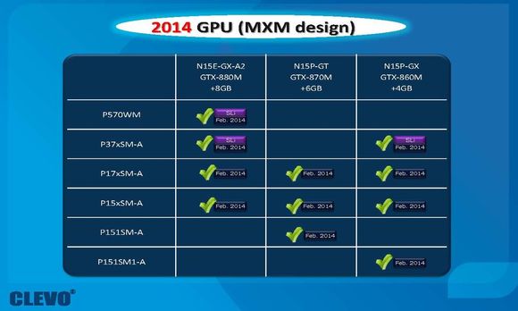
Look at P37xSM-A. It feature both 880M SLI and 860M SLI. Why should it have 8GB DDR3 on the 880M SLI model and 4GB DDR3 on the 860M SLI model?
- GTX 880M have 8GB VRAM according to a chinese reseller. That was already revealed way before I found the Clevo roadmap.
Taobao
Same with GTX 870M. It have 6GB VRAM like shown in the roadmap.
N15E-GS-A1 A2 GTX870M 6GB
It makes a ton more sense to have 8GB VRAM and 6GB VRAM because of the memory bandwidth, than changing the DDR3 on the machine according to the GPU. Atleast in my head
Today they posted results from a GPU blog run by a dude that have absolutely no idea about performance and basically just pulling numbers out of thin air. So wccftech and the rest are just posting whatever they find on the internet and writes a story about it mixed with their own opinions.
http://wccftech.com/nvidia-maxwell-800m-series-predicted-benchmarks-surface-compared-700m/ -
Ah, that's interesting Cloudfire, when I looked at it I initially thought that the link that Octiceps posted was a bonafide article rather than just a post. What you say makes sense, it would be silly to say only 880M systems get 8GB of system RAM and 870M systems can only have 6GB system RAM - that wouldn't make sense. I tend to agree with you that it's referring to the amount of VRAM. Still, it was a good find by Octiceps, I wonder where they got their info from that it was just referring to the system RAM. (Haha, and the content of that whole article does mirror the discussions & conclusions we've come to in parts of this thread - makes you wonder whether the creator of that post (article) really got his information from here!).
-
The closest thing we can look at to compare is:
GTX 670MX: 960 cores @ 600MHz. 192Bit. 24 ROPs
GTX 675MX: 960 cores @ 600MHz. 256bit. 32 ROPs
The 675MX is roughly 27% faster than GTX 670MX
Question is: Is it because of the ROP or is it bandwidth starved since they tested the cards maxed out on 1080p? -
Yup. I`ve seen several sites claiming Maxwell will have ARM and Unified Memory along with this information. It is fun to speculate and after all the sites do inform in the articles that it is not definitive proof but rumors.
Notebookreview listed 800M cards today btw and referred to this thread so they are indeed searching around for information.
NVIDIA GeForce GTX 880M - Notebookcheck.com Technik/FAQ
That update regarding DDR3, yeah who knows where they got it. Second thoughts by the author maybe? Can`t blame him, since the charts are a little confusing like octiceps says (GTX 880M +8GB) and not (GTX 880M 8GB GDDR5). 8GB VRAM is pretty hardcore compared to the Kepler`s we have today. Heck many are even running on 2GB VRAM. And now 8GB?! I think the chinese clevo reseller along with this information nudge it toward 8GB VRAM. In my opinion. After all, we have already K5100M with 8GB VRAM and to me it seems strange to change DDR3 according to the GPU. Atleast when its the same notebook model featuring it.Robbo99999 likes this. -
Notebookcheck is not accurate, as usual. Memory and core clock of the 675mx are about 13% higher than the ones of the 670mx, you need to consider this when comparing the cards.
670mx: 700MHz Memory, 601MHz core
675mx: 900MHz Memory, 667MHz core
For anything up to 1080p 6 or even 8GB is utter non-sense and complete overkill (unless for some very specific workstation applications.)
At 3k resolutions and more there are scenarios where the additional ram might help, but the upcoming GPUs will lack the power for gaming at resolutions with settings that would result in such a high vram usage.
Expect another rebadge round, or if Nvidia goes crazy then we might see a cut down GK110 chip, e.g. with 10SMX enabled. Though that would be a novelty, GK110 with 256bit bus. Currently I think that's the most likely option. -
Interesting. So considering that the 675MX runs on faster clocks and they tested with a faster CPU with the 675MX model, the ROPs might not have done that much to help performance then?
I thought about the GK110 option. There are several things that goes against it in my eyes.
GK110, Die size: 561 mm^2
Compare that with our 780M, which is 294mm^2. Are there really any room for that die with that size on current MXM boards? GK110 is almost double the size of a GK104.
I don`t think I have ever seen a die this big in notebooks before.
Memory interface on GK110 is 384bit. Our current MXM cards have a limit on 256bit right? Putting out GK110 with 256bit, wouldn`t that basically mean having to rebuild the chip?
I heard rumors about a 1920 core GPU releasing soon (10SMX) which could be our candidate, but it was said to have 384bit bus (GK110?) and 3GB VRAM (conflict with the 8GB information we have) -
GTX 880M
28nm GK110
10 SMX
1920 CUDA cores, 160 TMUs, 32 ROPs
671 MHz core, up to 820 MHz with GPU Boost 3.0
5400 MT/s memory
8GB 256-bit GDDR5 @ 172.8 GB/s
125 W TDP
-
Yes, I don't think that the ROPs matter a lot in this scenario, at least not at stock clocks in the most games where the fps aren't too high with these cards anyway.
I consider the die size argument invalid ever since the abomination called 480m, which was more a cooking plate than a working GPU... but it actually got released and sold:
 (thanks
@SFVogt for the nice pic)
(thanks
@SFVogt for the nice pic)
Die size roughly 530mm^2
The memory bus width can be adjusted with little effort.
I doubt that Nvidia is going to go the monster die way again after the 480m fiasco. Could be fun though. Besides, there was at least one mobile card with an even bigger chip if I'm not mistaken.
Cloudfire and Robbo99999 like this. -
The embedded 860m shows 2GB vRAM where the GTX version shows 4GB. It's all silliness until someone gets hurt.
-
Well yeah that one was a beast.
I don`t think its the size of the die itself that caused the temperatures of the 480M to get so insanely hot. I`m pretty sure the heatsinks and fans are big enough today to efficiently cool off a die like GK110 especially when Nvidia disable so many cores. I`m pretty sure 480M became hot because it was their first Fermi high end card and they messed up with the architecture and the scaling and such.
How can they change the bus width so easily btw? GK110 consist of 6 * 64bit memory controllers to make the 384bit bus. I have never seen them disable memory controllers to make the bus width smaller on an existing chip, but just disabling SMX`s. Here is GTX 780 and here is GTX Titan. All of them have the memory controllers untouched.
Are you sure they can just disable few of them without redesigning the core layout and such?
Atleast its not GDDR3 on the embedded one
-
670mx / 675mx say it's easy. 192bit vs 256 bit. Same principle.Cloudfire likes this.
-
Yep and don't forget 650 Ti vs. 650 Ti Boost (128-bit vs. 192-bit) and 660 Ti vs. 670 (192-bit vs. 256-bit). Lots of examples.Cloudfire likes this.
-
Good point
GTX 670MX is GK104, which should look like this.
That one have 4*64bit, 256bit memory bus, but GTX 670MX is actually 192bit.
Well that leave me a little more relieved. Maybe there will be GK110 with 10SMX`s after all? Still hope for Maxwell though and since our 8SMX (780M) is already touching the 100W limit, that GK110 better be efficient if they plan to
-
Notice that the GTX485M blasted past the 480M and no amount of tweaking could save the 480M.
The 780M would murder a cut down GK110 forced into a 100-125W envelope and missing a 3rd of its memory bandwidth and rop performance.
If the GTX670MX was so bandwidth starved it would scale linearly with memory clock and hardly any with core clock yet performance scales with the core more than the memory.sangemaru and Robbo99999 like this. -
Nothing new here but thought I would share anyways . ^^
NVIDIA GeForce GTX 880M - NotebookCheck.net Tech -
Lets look at it from both a historical and business perspectives..Nvidia never cannibalizes its top card, it rebrands a somehow worse version of the top card and makes that worse version the 2nd best..Here is what I mean:
2011:GTX 580 Top
2012 GTX 580 gets over-clocked becoming GTX 675M (Top card gone 2nd)
2012 GTX 680 is released, a new top card...
Since there is a huge gap they re-brand the previous top card (580) 2 more times as GTX 670MX, 675MX only in Kepler
2013 GTX 770 re-branded the 2012 top card but worsens it by decreasing from 256-192 and raising clock speeds..(about 7% decrease in performance)
Isn't the conclusion GTX 870=rebranded 256>192 worsened GTX 780 with raising clock speeds to make up?
Why are we expecting much more? Tech perspective offers hundreds of possibilities but business wise, it is looking grim for the customer... -
Because there were refresh that the top card get doubled performance?
680m "pwn" 770m real hard btw. -
The 675M was not an overclocked 580M
The 670MX and 675MX have no relation to the 580M
The 770M has no relation to the 680M
This has been the worst GPU history lesson of the day, one false connection after another. Nothing from the past leads to the conclusion that the 870M with be a 192-bit version of the 780M. Nvidia has never done such a thing.octiceps, Mr.Koala and Robbo99999 like this. -
LMAO this is so wrong.
-
CES 2014.
That is when there most likely will be official acknowledgement of the 800M series from Nvidia. Especially since Clevo are featuring them in their notebooks in February.
I remember CES 2012, Nvidia revealed GT 630M, their first Kepler card. Note that no other Kepler cards was announced.
GT 640M >>> GTX 660M was announced in late March. GTX 680M, their high end card was announced in early June. Just to give you guys a brief history on what happend on the Kepler launch back in 2012.
So keep an eye out for January 7-10th guys!reborn2003 likes this.
Clevo notebooks with 800M series coming out February 2014
Discussion in 'Gaming (Software and Graphics Cards)' started by Cloudfire, Dec 11, 2013.


